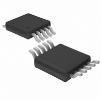
LT1618EMS Linear Technology, LT1618EMS Datasheet - Page 5

LT1618EMS
Manufacturer Part Number
LT1618EMS
Description
IC DC/DC CONV STEP-UP 10-MSOP
Manufacturer
Linear Technology
Type
Step-Up (Boost)r
Datasheet
1.LT1618EMSPBF.pdf
(16 pages)
Specifications of LT1618EMS
Internal Switch(s)
Yes
Synchronous Rectifier
No
Number Of Outputs
1
Voltage - Output
1.26 ~ 36 V
Current - Output
1.5A
Frequency - Switching
1.4MHz
Voltage - Input
1.6 ~ 18 V
Operating Temperature
-40°C ~ 85°C
Mounting Type
Surface Mount
Package / Case
10-MSOP, Micro10™, 10-uMAX, 10-uSOP
Lead Free Status / RoHS Status
Contains lead / RoHS non-compliant
Power - Output
-
Available stocks
Company
Part Number
Manufacturer
Quantity
Price
Company:
Part Number:
LT1618EMS
Manufacturer:
LT
Quantity:
10 000
Part Number:
LT1618EMS
Manufacturer:
LINEAR/凌特
Quantity:
20 000
Part Number:
LT1618EMS#PBF
Manufacturer:
LT/凌特
Quantity:
20 000
Part Number:
LT1618EMS8
Manufacturer:
LT/凌特
Quantity:
20 000
OPERATIO
The LT1618 uses a constant frequency, current mode
control scheme to provide excellent line and load regula-
tion. Operation can be best understood by referring to the
Block Diagram in Figure 1. At the start of each oscillator
cycle, the SR latch is set, turning on power switch Q1. The
signal at the noninverting input of PWM comparator A3 is
a scaled-down version of the switch current (summed
together with a portion of the oscillator ramp). When this
signal reaches the level set by the output of error amplifier
A2, comparator A3 resets the latch and turns off the power
switch. In this manner, A2 sets the correct peak current
level to keep the output in regulation. If the error amplifier’s
output increases, more current is delivered to the output;
if it decreases, less current is delivered. A2 has two
inverting inputs, one from the voltage feedback loop, and
one from the current feedback loop. Whichever inverting
BLOCK DIAGRA
V
IN
C1
9
SHDN
U
Q
8
DRIVER
V
5
IN
GND
R
S
W
L1
0.02Ω
OSCILLATOR
1.4MHz
7
Q1
SW
+
–
Figure 1. LT1618 Block Diagram
×5
A3
–
+
+
10
Σ
V
+
R
C
C
C
input is higher takes precedence, forcing the converter
into either a constant-current or a constant-voltage mode.
The LT1618 is designed to transition cleanly between the
two modes of operation. Current sense amplifier A1 senses
the voltage between the ISP and ISN pins and provides a
25× level-shifted version to error amplifier A2. When the
voltage between ISP and ISN reaches 50mV, the output of
A1 provides 1.263V to one of the noninverting inputs of A2
and the converter is in constant-current mode. If the
current sense voltage exceeds 50mV, the output of A1 will
increase causing the output of A2 to decrease, thus
reducing the amount of current delivered to the output. In
this manner the current sense voltage is regulated to
50mV. Similarly, if the FB pin increases above 1.263V, the
output of A2 will decrease to reduce the peak current level
and regulate the output (constant-voltage mode).
C
D1
A2
–
–
+
1.263V
×25
A1
–
+
3
2
4
1
ISP
ISN
FB
I
ADJ
C2
LT1618
R
SENSE
sn1618 1618fas
R1
R2
V
5
OUT


