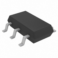
LTC3429BES6#TRPBF Linear Technology, LTC3429BES6#TRPBF Datasheet - Page 5

LTC3429BES6#TRPBF
Manufacturer Part Number
LTC3429BES6#TRPBF
Description
IC CONV DC/DC SYNC STPUPTSOT23-6
Manufacturer
Linear Technology
Type
Step-Up (Boost)r
Datasheet
1.LTC3429ES6TRMPBF.pdf
(12 pages)
Specifications of LTC3429BES6#TRPBF
Internal Switch(s)
Yes
Synchronous Rectifier
Yes
Number Of Outputs
1
Voltage - Output
2.5 ~ 4.3 V
Current - Output
600mA
Frequency - Switching
500kHz
Voltage - Input
0.5 ~ 4.4 V
Operating Temperature
-40°C ~ 85°C
Mounting Type
Surface Mount
Package / Case
TSOT-23-6, TSOT-6
Lead Free Status / RoHS Status
Lead free / RoHS Compliant
Power - Output
-
Available stocks
Company
Part Number
Manufacturer
Quantity
Price
BLOCK DIAGRA
PI FU CTIO S
SW (Pin 1): Switch Pin. Connect inductor between SW
and V
as possible to reduce EMI and voltage overshoot. If the
inductor current falls to zero, or SHDN is low, an internal
150Ω antiringing switch is connected from SW to V
minimize EMI.
GND (Pin 2): Signal and Power Ground. Provide a short
direct PCB path between GND and the (–) side of the output
capacitor(s).
FB (Pin 3): Feedback Input to the
Connect resistor divider tap to this pin. The output voltage
can be adjusted from 2.5V to 5V by:
SHDN (Pin 4): Logic Controlled Shutdown Input.
V
SHDN = High: Normal free running operation, 500kHz
typical operating frequency.
U
OUT
IN
. Keep these PCB trace lengths as short and wide
= 1.23V • [1 + (R1/R2)]
500kHz
RAMP
GEN
+
U
1V TO 4.4V
U
6
V
COMPARATOR
IN
SHDN
W
4
PWM
START-UP
SLEEP
OSC
+
–
–
SHUTDOWN
OPERATION
Burst Mode
CONTROL
CONTROL
CONTROL
g
SLOPE
COMP
m
PWM
Error Amplifier.
C
IN
A
B
MUX
A/B
IN
SHUTDOWN
to
R
80k
C
C
150pF
C
CONTROL
L1
DRIVE
SYNC
V
Internal Synchronous Rectifier MOSFET. Bias is derived
from V
capacitor(s) should be as short and wide as possible. V
is completely disconnected from V
due to the output disconnect feature.
V
start-up bias from V
comes from V
pletely independent from V
the output power level and the battery’s internal series
resistance.
GOOD
Σ
V
OUT
IN
OUT
SHDN = Low: Shutdown, quiescent current < 1µA.
Output capacitor can be completely discharged through
the load or feedback resistors. A 150Ω resistor is
internally connected between SW and V
C
2.5pF
+
–
P2
(Pin 6): Battery Input Voltage. The device gets its
(Pin 5): Output Voltage Sense Input and Drain of the
OUT
2.3V
. PCB trace length from V
1
2
0.45Ω
0.35Ω
CURRENT
SENSE
SW
GND
OUT
LTC3429/LTC3429B
. Thus, once started, operation is com-
ERROR
AMP
g
V
m
IN
WELL
SWITCH
–
+
IN
. Once V
(OPTIONAL)
IN
. Operation is only limited by
V
OUT
5
1.23V
C
REF
FB
PL
3
OUT
OUT
IN
2.5V TO 5V
when SHDN is low
exceeds V
to the output filter
R1
R2
IN
.
3429 BD
IN
C
OUT
, bias
3429fa
5
OUT


