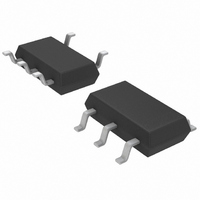
LTC3406ES5#TR Linear Technology, LTC3406ES5#TR Datasheet - Page 7

LTC3406ES5#TR
Manufacturer Part Number
LTC3406ES5#TR
Description
IC REG SYNC SDWN 1.5MHZ TSOT23-5
Manufacturer
Linear Technology
Type
Step-Down (Buck)r
Datasheet
1.LTC3406ES5TRMPBF.pdf
(16 pages)
Specifications of LTC3406ES5#TR
Internal Switch(s)
Yes
Synchronous Rectifier
Yes
Number Of Outputs
1
Voltage - Output
0.6 ~ 5.5 V
Current - Output
600mA
Frequency - Switching
1.5MHz
Voltage - Input
2.5 ~ 5.5 V
Operating Temperature
-40°C ~ 85°C
Mounting Type
Surface Mount
Package / Case
TSOT-23-5, TSOT-5, TSOP-5
Lead Free Status / RoHS Status
Contains lead / RoHS non-compliant
Power - Output
-
Other names
LTC3406ES5TR
Available stocks
Company
Part Number
Manufacturer
Quantity
Price
Short-Circuit Protection
When the output is shorted to ground, the frequency of the
oscillator is reduced to about 210kHz, 1/7 the nominal
frequency. This frequency foldback ensures that the in-
ductor current has more time to decay, thereby preventing
runaway. The oscillator’s frequency will progressively
increase to 1.5MHz when V
Dropout Operation
As the input supply voltage decreases to a value approach-
ing the output voltage, the duty cycle increases toward the
maximum on-time. Further reduction of the supply voltage
forces the main switch to remain on for more than one cycle
until it reaches 100% duty cycle. The output voltage will then
be determined by the input voltage minus the voltage drop
across the P-channel MOSFET and the inductor.
An important detail to remember is that at low input supply
voltages, the R
(see Typical Performance Characteristics). Therefore, the
user should calculate the power dissipation when the
LTC3406 is used at 100% duty cycle with low input voltage
(See Thermal Considerations in the Applications Informa-
tion section).
Low Supply Operation
The LTC3406 will operate with input supply voltages as
low as 2.5V, but the maximum allowable output current is
reduced at this low voltage. Figure 2 shows the reduction
OPERATIO
DS(ON)
U
(Refer to Functional Diagram)
of the P-channel switch increases
FB
or V
OUT
rises above 0V.
in the maximum output current as a function of input
voltage for various output voltages.
Slope Compensation and Inductor Peak Current
Slope compensation provides stability in constant fre-
quency architectures by preventing subharmonic oscilla-
tions at high duty cycles. It is accomplished internally by
adding a compensating ramp to the inductor current
signal at duty cycles in excess of 40%. Normally, this
results in a reduction of maximum inductor peak current
for duty cycles > 40%. However, the LTC3406 uses a
patent-pending scheme that counteracts this compensat-
ing ramp, which allows the maximum inductor peak
current to remain unaffected throughout all duty cycles.
Figure 2. Maximum Output Current vs Input Voltage
1200
1000
800
600
400
200
0
2.5
LTC3406-1.5/LTC3406-1.8
V
V
OUT
OUT
3.0
= 1.8V
= 1.5V
SUPPLY VOLTAGE (V)
3.5
V
OUT
4.0
= 2.5V
4.5
5.0
3406 F02
LTC3406
5.5
3406fa
7


