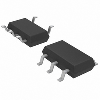
LTC3406BES5-1.2#TRM Linear Technology, LTC3406BES5-1.2#TRM Datasheet - Page 10

LTC3406BES5-1.2#TRM
Manufacturer Part Number
LTC3406BES5-1.2#TRM
Description
IC CNV 1.2V SYNC STPDWN TSOT23-5
Manufacturer
Linear Technology
Type
Step-Down (Buck)r
Datasheet
1.LTC3406BES5-1.2TRPBF.pdf
(12 pages)
Specifications of LTC3406BES5-1.2#TRM
Internal Switch(s)
Yes
Synchronous Rectifier
Yes
Number Of Outputs
1
Voltage - Output
1.2V
Current - Output
600mA
Frequency - Switching
1.5MHz
Voltage - Input
2.5 ~ 5.5 V
Operating Temperature
-40°C ~ 85°C
Mounting Type
Surface Mount
Package / Case
TSOT-23-5, TSOT-5, TSOP-5
Lead Free Status / RoHS Status
Contains lead / RoHS non-compliant
Power - Output
-
Other names
LTC3406BES5-1.2#TRMTR
Available stocks
Company
Part Number
Manufacturer
Quantity
Price
APPLICATIO S I FOR ATIO
LTC3406B-1.2
The regulator loop then acts to return V
state value. During this recovery time V
tored for overshoot or ringing that would indicate a stability
problem. For a detailed explanation of switching control
loop theory, see Application Note 76.
A second, more severe transient is caused by switching in
loads with large (>1µF) supply bypass capacitors. The
discharged bypass capacitors are effectively put in parallel
with C
deliver enough current to prevent this problem if the load
switch resistance is low and it is driven quickly. The only
solution is to limit the rise time of the switch drive so that
the load rise time is limited to approximately (25 • C
Thus, a 10µF capacitor charging to 3.3V would require a
250µs rise time, limiting the charging current to about
130mA.
PC Board Layout Checklist
When laying out the printed circuit board, the following
checklist should be used to ensure proper operation of the
LTC3406B-1.2. These items are also illustrated graphi-
cally in Figures 3 and 4. Check the following in your layout:
1. The power traces, consisting of the GND trace, the SW
2. Does the (+) plate of C
10
trace and the V
wide.
possible? This capacitor provides the AC current to the
internal power MOSFETs.
OUT
, causing a rapid drop in V
Figure 3. LTC3406B-1.2 Layout Diagram
V
OUT
–
+
BOLD LINES INDICATE HIGH CURRENT PATHS
IN
C
U
trace should be kept short, direct and
OUT
L1
1
2
3
U
IN
LTC3406B-1.2
RUN
SW
connect to V
GND
V
OUT
V
C
IN
IN
W
OUT
5
4
. No regulator can
OUT
OUT
IN
3406B12 F03
can be moni-
to its steady-
as closely as
V
IN
U
LOAD
).
3. Keep the (–) plates of C
Design Example
As a design example, assume the LTC3406B-1.2 is used
in a single lithium-ion battery-powered cellular phone
application. The V
4.2V down to about 2.7V. The load current requirement
is a maximum of 0.6A but most of the time it will be in
standby mode, requiring only 2mA. Efficiency at both low
and high load currents is important. With this informa-
tion we can calculate L using equation (1),
Substituting V
equation (3) gives:
A 2.2µH inductor works well for this application. For best
efficiency choose a 720mA or greater inductor with less
than 0.2Ω series resistance.
C
I
of less than 0.25Ω. In most cases, a ceramic capacitor will
satisfy this requirement.
LOAD(MAX)
IN
L
L
will require an RMS current rating of at least 0.3A ≅
=
=
V
OUT
1 5
( )
f
.
( )
Figure 4. LTC3406B-1.2 Suggested Layout
MHz
/2 at temperature and C
1
∆
I
L
1 2
IN
.
L1
(
1 2 1
240
V
= 4.2V, ∆I
.
IN
V
mA
will be operating from a maximum of
SW
⎛
⎜
⎝
PIN 1
−
C
)
OUT
⎛
⎜
⎝
IN
1 2
1
V
.
L
−
and C
IN
LTC3406B-1.2
V
= 240mA and f = 1.5MHz in
1 2
4 2
⎞
⎟
⎠
.
.
VIA TO V
GND
V
V
OUT
OUT
⎞
⎟ =
⎠
IN
as close as possible.
VIA TO V
will require an ESR
2 38
C
IN
.
OUT
sn3406b12 3406b12fs
µ
H
3406B12 F04
V
IN
(3)


