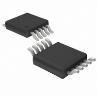
LTC3704IMS#PBF Linear Technology, LTC3704IMS#PBF Datasheet - Page 15

LTC3704IMS#PBF
Manufacturer Part Number
LTC3704IMS#PBF
Description
IC INV SYNC 5.2V 50MA 10MSOP
Manufacturer
Linear Technology
Type
Invertingr
Datasheet
1.LTC3704EMSPBF.pdf
(28 pages)
Specifications of LTC3704IMS#PBF
Internal Switch(s)
No
Synchronous Rectifier
No
Number Of Outputs
1
Voltage - Output
-5.2V
Current - Output
50mA
Frequency - Switching
50kHz ~ 1MHz
Voltage - Input
2.5 ~ 36 V
Operating Temperature
-40°C ~ 125°C
Mounting Type
Surface Mount
Package / Case
10-MSOP, Micro10™, 10-uMAX, 10-uSOP
Lead Free Status / RoHS Status
Lead free / RoHS Compliant
Power - Output
-
Available stocks
Company
Part Number
Manufacturer
Quantity
Price
APPLICATIO S I FOR ATIO
the initial equations for I
inductor is used, make sure that the minimum saturation
current for the parallel configuration exceeds the maxi-
mum switch current, or:
The saturation current rating should be checked at mini-
mum input voltage (which results in the highest average
inductor current) and maximum load current.
Operating in Discontinuous Mode
Discontinuous mode operation occurs when the load
current is low enough to allow the inductor current to run
out during the off-time of the switch, as shown in
Figure 10. Once the inductor current is near zero, the
switch and diode capacitances resonate with the induc-
tance to form damped ringing at 1MHz to 10MHz. If the
off-time is long enough, the drain voltage will settle to the
input voltage.
Depending on the input voltage and the residual energy in
the inductor, this ringing can cause the drain of the power
MOSFET to go below ground where it is clamped by the
body diode. This ringing is not harmful to the IC and it has
not been shown to contribute significantly to EMI. Any
attempt to damp it with a snubber will degrade the efficiency.
I
LSAT MIN
10V/DIV
1A/DIV
V
I
DS
L1
(
Figure 10. Discontinuous Mode Waveforms
(MODE/SYNC = INTV
for the Circuit in Figure 1.
V
NO LOAD
IN
)
= 15V
≥
–
⎛
⎜
⎝
1
U
+
χ
2
L1(PEAK)
⎞
⎟
⎠
1μs/DIV
U
•
I
CC
O MAX
(
, Pulse-Skip Mode)
and I
)
•
W
1
L2(PEAK)
–
D
1
MAX
3704 F10
. If a coupled
U
or
Power MOSFET or Sense Resistor Selection
If the maximum voltage on the drain of the power MOSFET
(which is V
36V then the circuit can take advantage of the LTC3704’s
No R
eliminate the sense resistor. For higher switch voltages
the SENSE pin should be connected to a resistor in the
source of the power MOSFET, as shown in Figure 2.
Internal leading-edge blanking is provided in the LTC3704
to eliminate the need for filtering components on the
SENSE pin.
In both positive-to-negative and flyback converters the
maximum switch current is equal to the input current plus
the output current. As a result, the peak switch current is:
where I
During the switch on-time, the control circuit limits the
maximum voltage drop across the power MOSFET to
150mV (at low duty cycles). The peak switch current is
therefore limited to 150mV/R
tween the maximum load current, the duty cycle and the
R
again, where I
term is typically 150mV at low duty cycle, and is reduced
to about 100mV at a duty cycle of 92% due to slope
compensation, as shown in Figure 11. The ρ
counts for the temperature coefficient of the R
MOSFET, which is typically 0.4%/°C. Figure 12 illustrates
the variation of R
power MOSFET (normalized for simplicity).
DS(ON)
I
R
R
SW PEAK
DS ON
DS ON
SENSE
(
(
(
O(MAX)
of the power MOSFET is:
)
)
IN(MAX)
technology in order to improve efficiency and
)
≤
≤
=
O(MAX)
V
V
is a negative number.
SENSE MAX
SENSE MAX
I
–
SW PEAK
⎛
⎜
⎝
1
+ V
DS(ON)
(
+
is a negative number. The V
(
(
OUT
χ
2
⎞
⎟
⎠
)
, plus any transients) is less than
•
)
over temperature for a typical
)
I
•
O MAX
⎛
⎜
⎝
(
DS(ON)
1
+
)
χ
2
•
D
⎞
⎟
⎠
. The relationship be-
1
MAX
•
–
I
O MAX
D
(
1
MAX
LTC3704
−
1
)
DS(ON)
•
SENSE(MAX)
Τ
ρ
term ac-
Τ
15
of the
3704fb


