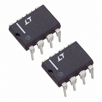
LTC1044AIN8 Linear Technology, LTC1044AIN8 Datasheet - Page 2

LTC1044AIN8
Manufacturer Part Number
LTC1044AIN8
Description
IC CMOS VOLT CONV SW-CAP 8-DIP
Manufacturer
Linear Technology
Type
Step-Up (Boost), Switched Capacitor (Charge Pump), Divider, Doubler, Invertingr
Datasheet
1.LTC1044ACN8.pdf
(12 pages)
Specifications of LTC1044AIN8
Internal Switch(s)
Yes
Synchronous Rectifier
No
Number Of Outputs
1
Current - Output
20mA
Frequency - Switching
1kHz ~ 5kHz
Voltage - Input
1.5 ~ 12 V
Operating Temperature
-40°C ~ 85°C
Mounting Type
Through Hole
Package / Case
8-DIP (0.300", 7.62mm)
Lead Free Status / RoHS Status
Contains lead / RoHS non-compliant
Voltage - Output
-
Power - Output
-
ABSOLUTE
LTC1044A
(Note 1)
Supply Voltage ........................................................ 13V
Input Voltage on Pins 1, 6 and 7
Current into Pin 6 ................................................. 20 A
Output Short-Circuit Duration
Operating Temperature Range
Storage Temperature Range ................ – 65 C to 150 C
Lead Temperature (Soldering, 10 sec)................. 300 C
SYMBOL
I
R
f
P
The
temperature range; all other limits and typicals T
Note 1: Absolute maximum ratings are those values beyond which the life
of a device may be impaired.
Note 2: Connecting any input terminal to voltages greater than V
than ground may cause destructive latch-up. It is recommended that no
2
ELECTRICAL C
S
OSC
EFF
OUT
V
LTC1044AC ............................................ 0 C to 70 C
LTC1044AI ........................................ – 40 C to 85 C
(Note 2) .............................. – 0.3V < V
+
denotes specifications which apply over the full operating
6.5V ................................................. Continuous
PARAMETER
Supply Current
Minimum Supply Voltage
Maximum Supply Voltage
Output Resistance
Oscillator Frequency
Power Efficiency
Voltage Conversion Efficiency
Oscillator Sink or Source
Current
W
AXI U
HARA TERISTICS
W W
C
CONDITIONS
R
R
V
R
R
I
V
V
V
R
R
V
Pin 1 (BOOST) = 0V
Pin 1 (BOOST) = V
L
OSC
L
L
L
L
L
L
+
+
+
+
A
= 20mA, f
= , Pins 1 and 7, No Connection
= , Pins 1 and 7, No Connection,
= 10k
= 10k
= 5k, f
=
= 3V
= 2V, I
= 5V, (Note 3)
= 2V
= 25 C.
RATI GS
= 0V or V
OSC
IN
L
= 3mA, f
OSC
< V
= 5kHz
U
+
= 5kHz
+
+
+
+ 0.3V
or less
OSC
V
+
= 5V, C
= 1kHz
OSC
PACKAGE/ORDER I FOR ATIO
Consult factory for Military grade parts
inputs from sources operating from external supplies be applied prior to
power-up of the LTC1044A.
Note 3: f
fixture capacitance loading. The 0pF frequency is correlated to this 100pF
test point, and is intended to simulate the capacitance at pin 7 when the
device is plugged into a test socket and no external capacitor is used.
= 0pF, T
BOOST
BOOST
CAP
CAP
CAP
CAP
GND
GND
OSC
+
–
+
–
T
T
JMAX
JMAX
A
is tested with C
8-LEAD PLASTIC SOIC
1
2
3
4
1
2
3
4
8-LEAD PLASTIC DIP
= 25 C, See Test Circuit, unless otherwise noted.
= 110 C,
= 110 C,
N8 PACKAGE
S8 PACKAGE
MIN
1.5
95
97
TOP VIEW
TOP VIEW
5
1
LTC1044AC
JA
JA
99.9
= 100 C/W
= 130 C/W
TYP
60
15
98
OSC
8
7
6
5
8
7
6
5
= 100pF to minimize the effects of test
V
OSC
LV
V
V
OSC
LV
V
OUT
MAX MIN
+
200
100
120
310
+
OUT
12
20
3
U
1.5
95
97
5
1
S8 PART MARKING
LTC1044AI
LTC1044ACS8
LTC1044AIS8
LTC1044ACN8
LTC1044AIN8
ORDER PART
ORDER PART
99.9
TYP
60
15
98
NUMBER
NUMBER
W
1044A
1044AI
MAX
200
100
130
325
12
20
3
UNITS
U
kHz
kHz
%
%
A
A
V
V
A
A


