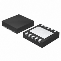
LT3757EDD#TRPBF Linear Technology, LT3757EDD#TRPBF Datasheet - Page 15

LT3757EDD#TRPBF
Manufacturer Part Number
LT3757EDD#TRPBF
Description
IC CTRLR DC/DC ADJ 10-DFN
Manufacturer
Linear Technology
Type
Step-Up (Boost), Inverting, Flyback, Sepicr
Datasheet
1.LT3757EDDPBF.pdf
(36 pages)
Specifications of LT3757EDD#TRPBF
Internal Switch(s)
No
Synchronous Rectifier
No
Number Of Outputs
1
Frequency - Switching
100kHz ~ 1MHz
Voltage - Input
2.9 ~ 40 V
Operating Temperature
-40°C ~ 125°C
Mounting Type
Surface Mount
Package / Case
10-DFN
Lead Free Status / RoHS Status
Lead free / RoHS Compliant
Current - Output
-
Voltage - Output
-
Power - Output
-
Available stocks
Company
Part Number
Manufacturer
Quantity
Price
applicaTions inForMaTion
Boost Converter: Inductor and Sense Resistor Selection
For the boost topology, the maximum average inductor
current is:
Then, the ripple current can be calculated by:
The constant c in the preceding equation represents the
percentage peak-to-peak ripple current in the inductor,
relative to I
The inductor ripple current has a direct effect on the choice
of the inductor value. Choosing smaller values of ∆I
requires large inductances and reduces the current loop
gain (the converter will approach voltage mode). Accepting
larger values of ∆I
allows the use of low inductances, but results in higher input
current ripple and greater core losses. It is recommended
that c fall within the range of 0.2 to 0.6.
Given an operating input voltage range, and having chosen
the operating frequency and ripple current in the inductor,
the inductor value of the boost converter can be determined
using the following equation:
The peak and RMS inductor current are:
I
L
I
I
∆I
L MAX
L PEAK
L RMS
(
=
(
(
L
V
=
∆
IN MIN
c
)
I
)
)
(
L
=
=
•
L(MAX)
=
•
I
I
I
L MAX
I
O MAX
L MAX
f
L MAX
(
(
)
(
(
•
D
.
MAX
L
)
)
)
provides fast transient response and
)
=
•
•
•
1
c
−
1
1 1
•
+
+
D
I
1
O MAX
MAX
c
(
2
c
12
2
)
•
1
−
D
1
MAX
L
Based on these equations, the user should choose the
inductors having sufficient saturation and RMS current
ratings.
Set the sense voltage at I
SENSE current limit threshold with a 20% margin. The
sense resistor value can then be calculated to be:
Boost Converter: Power MOSFET Selection
Important parameters for the power MOSFET include the
drain-source voltage rating (V
(V
and gate to drain charges (Q
drain current (I
resistances (R
The power MOSFET will see full output voltage, plus a
diode forward voltage, and any additional ringing across
its drain-to-source during its off-time. It is recommended
to choose a MOSFET whose B
a safety margin (a 10V safety margin is usually sufficient).
The power dissipated by the MOSFET in a boost converter is:
P
• C
The first term in the preceding equation represents the
conduction losses in the device, and the second term, the
switching loss. C
which is usually specified in the MOSFET characteristics.
For maximum efficiency, R
minimized. From a known power dissipated in the power
MOSFET, its junction temperature can be obtained using
the following equation:
T
GS(TH)
R
J
FET
SENSE
= T
RSS
= I
), the on-resistance (R
A
• f / 1A
+ P
2
=
L(MAX)
I
L PEAK
80
FET
θJC
(
mV
• θ
RSS
D(MAX)
and R
• R
)
JA
is the reverse transfer capacitance,
DS(ON)
= T
θJA
) and the MOSFET’s thermal
L(PEAK)
A
+ P
).
• D
DS(ON)
GS
VDSS
DS
DS(ON)
FET
to be the minimum of the
and Q
MAX
), the threshold voltage
• (θ
is higher than V
and C
+ 2 • V
), the gate to source
GD
JC
+ θ
), the maximum
RSS
2
LT3757
OUT
CA
should be
)
• I
L(MAX)
OUT
3757fb
by


