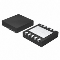
LT3437EDD#PBF Linear Technology, LT3437EDD#PBF Datasheet - Page 24

LT3437EDD#PBF
Manufacturer Part Number
LT3437EDD#PBF
Description
IC REG SW HV 500MA 10-DFN
Manufacturer
Linear Technology
Type
Step-Down (Buck)r
Datasheet
1.LT3437HFEPBF.pdf
(28 pages)
Specifications of LT3437EDD#PBF
Internal Switch(s)
Yes
Synchronous Rectifier
No
Number Of Outputs
1
Voltage - Output
1.25 ~ 54 V
Current - Output
500mA
Frequency - Switching
200kHz
Voltage - Input
3.3 ~ 60 V
Operating Temperature
-40°C ~ 125°C
Mounting Type
Surface Mount
Package / Case
10-DFN
Dc To Dc Converter Type
Step Down
Pin Count
10
Input Voltage
60V
Output Voltage
1.25 to 54V
Switching Freq
240KHz
Output Current
500mA
Package Type
DFN EP
Output Type
Adjustable
Switching Regulator
Yes
Mounting
Surface Mount
Input Voltage (min)
3.3V
Operating Temp Range
-40C to 125C
Operating Temperature Classification
Automotive
Lead Free Status / RoHS Status
Lead free / RoHS Compliant
Power - Output
-
Lead Free Status / Rohs Status
Compliant
Available stocks
Company
Part Number
Manufacturer
Quantity
Price
LT3437
APPLICATIO S I FOR ATIO
24
C
A zero can be added into the loop by placing a resistor (R
at the V
or by placing a capacitor (C
FB pin.
When using R
First, the combination of output capacitor ESR and R
stop the loop rolling off altogether. Second, if the loop gain
is not rolled off sufficiently at the switching frequency,
output ripple will perturb the V
unstable duty cycle switching, similar to subharmonic
oscillations. If needed, an additional capacitor (C
added across the R
to further suppress V
With a tantalum output capacitor, the LT3437 already
includes a resistor (R
pin (see Figures 10 and 11) to compensate the loop over
the entire V
R
C
C
C
F
C
pin in series with the compensation capacitor, C
LT3437
IN
Figure 10. Model for Loop Response
V
CURRENT MODE
POWER STAGE
C
range (to allow for stable pulse skipping for
C
g
, the maximum value has two limitations.
m
= 1
U
C
Ω
/C
g
1.6M
m
C
C
C
= 650µ
) and filter capacitor (C
ripple voltage.
network from the V
U
ERROR
FB
Ω
AMP
) between the output and the
–
+
C
W
pin enough to cause
1.25V
SW
FB
R1
R2
C
pin to ground
F
U
) at the V
F
3437 F13
C
) can be
FB
C
may
ESR
C
OUTPUT
OUT
C
C
C
)
,
high V
can still be used with a simple adjustment to the resistor R
for stable operation (see Ceramic Capacitors section for
stabilizing LT3430). If additional phase margin is required,
a capacitor (C
FB pin, but care must be taken for high output voltage
applications. Sudden shorts to the output can create
unacceptably large negative transients on the FB pin.
For V
possible by readjusting the frequency compensation com-
ponents at the V
When checking loop stability, the circuit should be oper-
ated over the application’s full voltage, current and tem-
perature range. Proper loop compensation may be obtained
by empirical methods, as described in Application Notes
19 and 76.
IN
IN
-to-V
-to-V
–40
100
–20
80
60
40
20
0
OUT
10
OUT
Figure 11. Overall Loop Response
FB
) can be inserted between the output and
C
ratios < 10, higher loop bandwidths are
ratios ≥ 10). A ceramic output capacitor
100
pin.
FREQUENCY (Hz)
1k
V
C
C
R
C
I
10k
LOAD
OUT
OUT
F
C
C
= 330pF
= 25k
= 1500pF
= 3.3V
= 100µF, 0.1Ω
= 250mA
100k
3437 F12
1M
0
–20
–40
–60
–80
–100
–120
–140
–160
–180
3437fc
C


