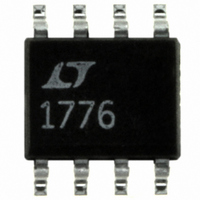
LT1776CS8 Linear Technology, LT1776CS8 Datasheet - Page 7

LT1776CS8
Manufacturer Part Number
LT1776CS8
Description
IC SW REG STEP-DOWN HI-EFF 8SOIC
Manufacturer
Linear Technology
Type
Step-Down (Buck)r
Datasheet
1.LT1776CS8PBF.pdf
(20 pages)
Specifications of LT1776CS8
Internal Switch(s)
Yes
Synchronous Rectifier
No
Number Of Outputs
1
Voltage - Output
1.24 ~ 34 V
Current - Output
700mA
Frequency - Switching
200kHz
Voltage - Input
7.4 ~ 40 V
Operating Temperature
0°C ~ 125°C
Mounting Type
Surface Mount
Package / Case
8-SOIC (3.9mm Width)
Lead Free Status / RoHS Status
Contains lead / RoHS non-compliant
Power - Output
-
Available stocks
Company
Part Number
Manufacturer
Quantity
Price
Part Number:
LT1776CS8
Manufacturer:
LINEAR/凌特
Quantity:
20 000
Part Number:
LT1776CS8#PBF
Manufacturer:
LT/凌特
Quantity:
20 000
Part Number:
LT1776CS8#TRPBF
Manufacturer:
LINEAR/凌特
Quantity:
20 000
OPERATIO
The LT1776 is a current mode switching regulator IC that
has been optimized for high efficiency operation in high
input voltage, low output voltage buck topologies. The
Block Diagram shows an overall view of the system.
Several of the blocks are straightforward and similar to
those found in traditional designs, including: Internal Bias
Regulator, Oscillator and Feedback Amplifier. The novel
portion includes an elaborate Output Switch section and
Logic Section to provide the control signals required by
the switch section.
The LT1776 operates much the same as traditional
current mode switchers, the major difference being its
specialized output switch section. Due to space con-
straints, this discussion will not reiterate the basics of
current mode switcher/controllers and the “buck” topol-
ogy. A good source of information on these topics is
Application Note 19.
Output Switch Theory
One of the classic problems in delivering low output
voltage from high input voltage at good efficiency is that
minimizing AC switching losses requires very fast volt-
age (dV/dt) and current (dI/dt) transition at the output
device. This is in spite of the fact that in a bipolar
implementation, slow lateral PNPs must be included in
the switching signal path.
TIMING DIAGRAMS
W U
SWOFF
BOOST
SWDR
SWON
V
SW
V
IN
0
U
High dV/dt Mode
W
1776 TD01
Fast positive-going slew rate action is provided by lateral
PNP Q3 driving the Darlington arrangement of Q1 and Q2.
The extra
requirements of Q3.
Although desirable for dynamic reasons, this topology
alone will yield a large DC forward voltage drop. A second
lateral PNP, Q4, acts directly on the base of Q1 to reduce
the voltage drop after the slewing phase has taken place.
To achieve the desired high slew rate, PNPs Q3 and Q4 are
“force-fed” packets of charge via the current sources
controlled by the boost signal.
Please refer to the High dV/dt Mode Timing Diagram. A
typical oscillator cycle is as follows: The logic section first
generates an SWDR signal that powers up the current
comparator and allows it time to settle. About 1 s later, the
SWON signal is asserted and the BOOST signal is pulsed
for a few hundred nanoseconds. After a short delay, the
V
current indicated by the control voltage V
reached (current mode control), the SWON and SWDR
signals are turned off, and SWOFF is pulsed for several
hundred nanoseconds. The use of an explicit turn-off
device, i.e., Q5, improves turn-off response time and thus
aids both controllability and efficiency.
SW
pin slews rapidly to V
SWOFF
BOOST
SWDR
SWON
V
SW
V
IN
0
available from Q2 greatly reduces the drive
Low dV/dt Mode
IN
. Later, after the peak switch
LT1776
C
has been
1776 TD02
7


