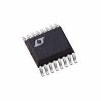
LTC1778EGN Linear Technology, LTC1778EGN Datasheet - Page 7

LTC1778EGN
Manufacturer Part Number
LTC1778EGN
Description
IC CONTROLLR STP-DWN SYNC 16SSOP
Manufacturer
Linear Technology
Type
Step-Down (Buck)r
Datasheet
1.LTC1778EGNPBF.pdf
(24 pages)
Specifications of LTC1778EGN
Internal Switch(s)
No
Synchronous Rectifier
Yes
Number Of Outputs
1
Current - Output
2A
Voltage - Input
4 ~ 36 V
Operating Temperature
-40°C ~ 85°C
Mounting Type
Surface Mount
Package / Case
16-SSOP
Lead Free Status / RoHS Status
Contains lead / RoHS non-compliant
Voltage - Output
-
Power - Output
-
Frequency - Switching
-
Available stocks
Company
Part Number
Manufacturer
Quantity
Price
Part Number:
LTC1778EGN
Manufacturer:
LT/凌特
Quantity:
20 000
Part Number:
LTC1778EGN#PBF
Manufacturer:
LINEAR/凌特
Quantity:
20 000
Company:
Part Number:
LTC1778EGN#TRPBF
Manufacturer:
MAXIM
Quantity:
1 351
Part Number:
LTC1778EGN#TRPBF
Manufacturer:
LINEAR/凌特
Quantity:
20 000
Company:
Part Number:
LTC1778EGN-1
Manufacturer:
Linear Technology
Quantity:
1 992
Company:
Part Number:
LTC1778EGN-1
Manufacturer:
LT
Quantity:
10 000
Part Number:
LTC1778EGN-1
Manufacturer:
LT/凌特
Quantity:
20 000
Part Number:
LTC1778EGN-1#TRPBF
Manufacturer:
LINEAR/凌特
Quantity:
20 000
Company:
Part Number:
LTC1778EGN-TR
Manufacturer:
LINEAR
Quantity:
2 897
PI FU CTIO S
RUN/SS (Pin 1): Run Control and Soft-Start Input. A
capacitor to ground at this pin sets the ramp time to full
output current (approximately 3s/µF) and the time delay
for overcurrent latchoff (see Applications Information).
Forcing this pin below 0.8V shuts down the device.
PGOOD (Pin 2, LTC1778): Power Good Output. Open
drain logic output that is pulled to ground when the output
voltage is not within ±7.5% of the regulation point.
V
trip point for the on-time comparator. Tying this pin to the
output voltage or an external resistive divider from the
output makes the on-time proportional to V
comparator input defaults to 0.7V when the pin is grounded
or unavailable (LTC1778) and defaults to 2.4V when the
pin is tied to INTV
applications to use a lower R
V
this pin is ten times the nominal sense voltage at maxi-
mum output current and can be set from 0.5V to 2V by a
resistive divider from INTV
defaults to 70mV when this pin is tied to ground, 140mV
when tied to INTV
FCB (Pin 4): Forced Continuous Input. Tie this pin to
ground to force continuous synchronous operation at low
load, to INTV
at low load or to a resistive divider from a secondary output
when using a secondary winding.
I
Compensation Point. The current comparator threshold
increases with this control voltage. The voltage ranges
from 0V to 2.4V with 0.8V corresponding to zero sense
voltage (zero current).
SGND (Pin 6): Signal Ground. All small-signal compo-
nents and compensation components should connect to
this ground, which in turn connects to PGND at one point.
TH
ON
RNG
U
(Pin 5): Current Control Threshold and Error Amplifier
(Pin 2, LTC1778-1): On-Time Voltage Input. Voltage
(Pin 3): Sense Voltage Range Input. The voltage at
U
CC
to enable discontinuous mode operation
CC
CC
U
.
. Tie this pin to INTV
CC
. The nominal sense voltage
ON
value.
CC
in high V
OUT
. The
OUT
I
to this pin to set the one-shot timer current and thereby set
the switching frequency.
V
connects the error amplifier input to an external resistive
divider from V
EXTV
ceeds 4.7V, an internal switch connects this pin to INTV
and shuts down the internal regulator so that controller
and gate drive power is drawn from EXTV
7V at this pin and ensure that EXTV
V
PGND with an RC filter (1Ω, 0.1µF).
INTV
and control circuits are powered from this voltage. De-
couple this pin to power ground with a minimum of 4.7µF
low ESR tantalum capacitor.
BG (Pin 12): Bottom Gate Drive. Drives the gate of the
bottom N-channel MOSFET between ground and INTV
PGND (Pin 13): Power Ground. Connect this pin closely to
the source of the bottom N-channel MOSFET, the (–)
terminal of C
SW (Pin 14): Switch Node. The (–) terminal of the boot-
strap capacitor C
diode voltage drop below ground up to V
TG (Pin 15): Top Gate Drive. Drives the top N-channel
MOSFET with a voltage swing equal to INTV
posed on the switch node voltage SW.
BOOST (Pin 16): Boosted Floating Driver Supply. The (+)
terminal of the bootstrap capacitor C
pin swings from a diode voltage drop below INTV
V
ON
FB
IN
IN
(Pin 7): On-Time Current Input. Tie a resistor from V
+ INTV
(Pin 10): Main Input Supply. Decouple this pin to
(Pin 8): Error Amplifier Feedback Input. This pin
CC
CC
(Pin 11): Internal 5V Regulator Output. The driver
(Pin 9): External V
CC
VCC
.
OUT
and the (–) terminal of C
B
.
connects here. This pin swings from a
LTC1778/LTC1778-1
CC
Input. When EXTV
CC
B
connects here. This
< V
CC
IN
IN
IN
. Do not exceed
.
.
.
CC
superim-
CC
CC
up to
1778fb
7
ex-
CC
CC
IN
.


