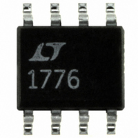
LT1776CS8#TR Linear Technology, LT1776CS8#TR Datasheet - Page 10

LT1776CS8#TR
Manufacturer Part Number
LT1776CS8#TR
Description
IC REG SW STEPDOWN HI EFF 8SOIC
Manufacturer
Linear Technology
Type
Step-Down (Buck)r
Datasheet
1.LT1776CS8PBF.pdf
(20 pages)
Specifications of LT1776CS8#TR
Internal Switch(s)
Yes
Synchronous Rectifier
No
Number Of Outputs
1
Voltage - Output
1.24 ~ 34 V
Current - Output
700mA
Frequency - Switching
200kHz
Voltage - Input
7.4 ~ 40 V
Operating Temperature
0°C ~ 125°C
Mounting Type
Surface Mount
Package / Case
8-SOIC (3.9mm Width)
Lead Free Status / RoHS Status
Contains lead / RoHS non-compliant
Power - Output
-
Available stocks
Company
Part Number
Manufacturer
Quantity
Price
LT1776
APPLICATIONS
Input Voltage vs Operating Frequency Considerations
The absolute maximum input supply voltage for the LT1776
is specified at 60V. This is based solely on internal semi-
conductor junction breakdown effects. Due to internal
power dissipation, the actual maximum V
a particular application may be less than this.
A detailed theoretical basis for estimating internal power
loss is given in the section, Thermal Considerations. Note
that AC switching loss is proportional to both operating
frequency and output current. The majority of AC switch-
ing loss is also proportional to the square of input voltage.
For example, while the combination of V
5V at 500mA and f
simultaneously raising V
not possible. Nevertheless, input voltage transients up to
60V can usually be accommodated, assuming the result-
ing increase in internal dissipation is of insufficient time
duration to raise die temperature significantly.
A second consideration is controllability. A potential limi-
tation occurs with a high step-down ratio of V
as this requires a correspondingly narrow minimum switch
ON time. An approximate expression for this (assuming
continuous mode operation) is given as follows:
where:
V
V
V
f
It is important to understand the nature of minimum
switch ON time as given in the data sheet. This test is
intended to mimic behavior under short-circuit condi-
tions. It is performed with the V
clamp level (V
to ground for simplicity. The resulting ON time behavior is
overconservative as a general operating design value for
two reasons. First, actual power supply application cir-
cuits present an inductive load to the V
10
OSC
IN
OUT
F
M
= Schottky diode forward drop
= input voltage
= switching frequency
in t
= output voltage
ON
CL
V
V f
OUT
IN OSC
) and uses a fixed resistive load from V
OSC
U
V
= 200kHz may be easily achievable,
F
INFORMATION
IN
U
to 60V and f
C
W
control voltage at its
OSC
IN
IN
SW
= 40V, V
achievable in
to 400kHz is
IN
node. The
U
to V
OUT
OUT
SW
=
,
Burst Mode is a trademark of Linear Technology Corporation.
resulting ramping current behavior helps overdrive the
current comparator (current mode switching) and reduce
its propagation delay, hastening output switch turnoff.
Second, and more importantly, actual power supply op-
eration involves a feedback amplifier that adjusts the V
node control voltage to maintain proper output voltage. As
progressively shorter ON times are required, the feedback
loop acts to reduce V
reduces the propagation delay in the current comparator.
A suggested worst-case limit for minimum switch ON time
in actual operation is 350ns.
A potential controllability problem arises if the LT1776 is
called upon to produce an ON time shorter than its ability.
Feedback loop action will lower then reduce the V
voltage to the point where some sort of cycle-skipping or
odd/even cycle behavior is exhibited.
In summary:
1. Be aware that the simultaneous requirements of high
2. The simultaneous requirements of high V
Minimum Load Considerations
As discussed previously, a lightly loaded LT1776 with V
pin control voltage below the boost threshold will operate
in low dV/dt mode. This affords greater controllability at
light loads, as minimum t
However, some users may be indifferent to pulse skipping
behavior, but instead may be concerned with maintaining
maximum possible efficiency at light loads. This require-
ment can be satisfied by forcing the part into Burst Mode
operation. The use of an external comparator whose
V
practice due to internal dissipation. The Thermal Con-
siderations section offers a basis to estimate internal
power. In questionable cases a prototype supply should
be built and exercised to verify acceptable operation.
and high f
minimum switch ON time. Cycle skipping and/or odd/
even cycle behavior will result although correct output
voltage is usually maintained.
IN
, high I
OUT
OSC
and high f
can result in an unacceptably short
C
, and the resulting overdrive further
ON
OSC
requirements are relaxed.
may not be achievable in
IN
, low V
C
control
OUT
TM
C
C


