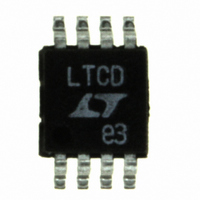
LT1316CMS8 Linear Technology, LT1316CMS8 Datasheet - Page 5

LT1316CMS8
Manufacturer Part Number
LT1316CMS8
Description
IC DC/DC CONVRTR STEP-UP 8-MSOP
Manufacturer
Linear Technology
Type
Step-Up (Boost)r
Datasheet
1.LT1316CS8PBF.pdf
(16 pages)
Specifications of LT1316CMS8
Internal Switch(s)
Yes
Synchronous Rectifier
No
Number Of Outputs
1
Voltage - Output
1.23 ~ 30 V
Current - Output
500mA
Voltage - Input
1.5 ~ 12 V
Operating Temperature
0°C ~ 70°C
Mounting Type
Surface Mount
Package / Case
8-MSOP, Micro8™, 8-uMAX, 8-uSOP,
Lead Free Status / RoHS Status
Contains lead / RoHS non-compliant
Power - Output
-
Frequency - Switching
-
Available stocks
Company
Part Number
Manufacturer
Quantity
Price
Company:
Part Number:
LT1316CMS8
Manufacturer:
LT
Quantity:
10 000
Part Number:
LT1316CMS8
Manufacturer:
LINEAR/凌特
Quantity:
20 000
Part Number:
LT1316CMS8#PBF
Manufacturer:
LT凌特厂
Quantity:
20 000
Company:
Part Number:
LT1316CMS8#TR
Manufacturer:
LT
Quantity:
1 000
Company:
Part Number:
LT1316CMS8#TRPBF
Manufacturer:
AMI
Quantity:
6 219
Part Number:
LT1316CMS8#TRPBF
Manufacturer:
LINEAR/凌特
Quantity:
20 000
LBO (Pin 1): Low-Battery Detector Output. Open collector
can sink up to 500 A. Low-battery detector remains active
in shutdown mode.
LBI (Pin 2): Low-Battery Detector Input. When voltage at
this pin drops below 1.17V, LBO goes low.
R
peak switch current. The resistor value should be between
3k and 150k. Do not float or short to ground. This is a high
impedance node. Keep traces at this pin as short as
possible. Do not put capacitance at this pin.
GND (Pin 4): Ground. Connect directly to ground plane.
BLOCK DIAGRA
PIN
SET
LBI
U
(Pin 3): A resistor between R
2
FUNCTIONS
1.17V
U
+
–
LB0
1
0.5V
A3
U
UNDERVOLTAGE
+
–
W
LOCKOUT
A4
1.5V
SET
V
IN
and GND programs
6
3
R3 = 10R4
R5
V
R
IN
SET
Figure 1. LT1316 Block Diagram
+
A2
–
L1
Q2
1
4
R4
GND
200
SW (Pin 5): Collector of NPN Power Transistor. Keep
traces at this pin as short as possible.
V
pin.
SHDN (Pin 7): Shutdown. Ground this pin to place the part
in shutdown mode (only the low-battery detector remains
active). Tie to a voltage between 1.4V and 6V to enable the
device. SHDN pin is logic level and need only meet the
logic specification (1.4V for high, 0.4V for low).
FB (Pin 8): Feedback Pin. Reference voltage is 1.23V.
Connect resistive divider tap here. Minimize trace area at
FB. Set V
Q1
IN
5
(Pin 6): Input Supply. Must be bypassed close to the
SW
DRIVER
OUT
according to: V
D1
OSCILLATOR
6.3 s ON
2 s OFF
SHDN
OUT
A1
7
C1
–
+
= 1.23V(1 + R1/R2).
V
1.23V
REF
1316 F01
8
LT1316
FB
R1
R2
V
OUT
5


