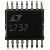
LT1737CGN#PBF Linear Technology, LT1737CGN#PBF Datasheet - Page 10

LT1737CGN#PBF
Manufacturer Part Number
LT1737CGN#PBF
Description
IC CTRLR ISOLATED FLYBACK 16SSOP
Manufacturer
Linear Technology
Type
Flybackr
Datasheet
1.LT1737IGNPBF.pdf
(28 pages)
Specifications of LT1737CGN#PBF
Internal Switch(s)
No
Synchronous Rectifier
No
Number Of Outputs
1
Frequency - Switching
50kHz ~ 250kHz
Voltage - Input
4.1 ~ 20 V
Operating Temperature
0°C ~ 100°C
Mounting Type
Surface Mount
Package / Case
16-SSOP
Primary Input Voltage
20V
No. Of Outputs
1
Output Voltage
12.1V
Output Current
100mA
No. Of Pins
16
Operating Temperature Range
0°C To +100°C
Msl
MSL 1 - Unlimited
Rohs Compliant
Yes
Lead Free Status / RoHS Status
Lead free / RoHS Compliant
Current - Output
-
Voltage - Output
-
Power - Output
-
Available stocks
Company
Part Number
Manufacturer
Quantity
Price
OPERATIO
LT1737
Enable Delay
When the output switch shuts off, the flyback pulse
appears. However, it takes a finite time until the trans-
former primary side voltage waveform approximately rep-
resents the output voltage. This is partly due to finite rise
time on the MOSFET drain node, but more importantly,
due to transformer leakage inductance. The latter causes
a voltage spike on the primary side not directly related to
output voltage. (Some time is also required for internal
settling of the feedback amplifier circuitry.)
In order to maintain immunity to these phenomena, a fixed
delay is introduced between the switch turnoff command
and the enabling of the feedback amplifier. This is termed
enable delay. In certain cases where the leakage spike is
not sufficiently settled by the end of the enable delay
period, regulation error may result. See Application Infor-
mation for further details.
Collapse Detect
Once the feedback amplifier is enabled, some mechanism
is then required to disable it. This is accomplished by a
collapse detect comparator, which compares the flyback
voltage (FB referred) to a fixed reference, nominally 80%
of V
level, the feedback amplifier is disabled. This action
accommodates both continuous and discontinuous mode
operation.
10
BG
. When the flyback waveform drops below this
U
R1
R2
COMP I
FB
LOAD
Q1 Q2
I
M
Figure 1. Load Compensation Diagram
V
BG
I
M
Q3
R
OCMP
A1
Minimum Enable Time
The feedback amplifier, once enabled, stays enabled for a
fixed minimum time period termed “minimum enable
time.” This prevents lockup, especially when the output
voltage is abnormally low, e.g., during start-up. The mini-
mum enable time period ensures that the V
to “pump up” and increase the current mode trip point to
the level where the collapse detect system exhibits proper
operation. The “minimum enable time” often determines
the low load level at which output voltage regulation is lost.
See Applications Information for details.
Effects of Variable Enable Period
It should now be clear that the flyback amplifier is enabled
during only a portion of the cycle time. This can vary from
the fixed “minimum enable time” described to a maximum
of roughly the “off” switch time minus the enable delay
time. Certain parameters of flyback amp behavior will then
be directly affected by the variable enable period. These
include effective transconductance and V
LOAD COMPENSATION THEORY
The LT1737 uses the flyback pulse to obtain information
about the isolated output voltage. A potential error source
is caused by transformer secondary current flow through
the real life nonzero impedances of the output rectifier,
+
–
R
CMPC
50k
R3
I
SENSE
V
IN
M1
R
1737 F01
SENSE
T1
C
node slew rate.
C
node is able
1737fa


