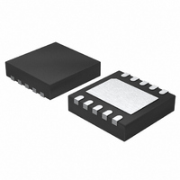
LTC3407EDD-2 Linear Technology, LTC3407EDD-2 Datasheet - Page 11

LTC3407EDD-2
Manufacturer Part Number
LTC3407EDD-2
Description
IC REG DC/DC DUAL STEPDOWN 10DFN
Manufacturer
Linear Technology
Type
Step-Down (Buck)r
Datasheet
1.LTC3407EDD-2.pdf
(16 pages)
Specifications of LTC3407EDD-2
Internal Switch(s)
Yes
Synchronous Rectifier
Yes
Number Of Outputs
2
Voltage - Output
0.6 ~ 5 V
Current - Output
1A
Frequency - Switching
1.5MHz
Voltage - Input
2.5 ~ 5.5 V
Operating Temperature
-40°C ~ 85°C
Mounting Type
Surface Mount
Package / Case
10-DFN
Lead Free Status / RoHS Status
Contains lead / RoHS non-compliant
Power - Output
-
Available stocks
Company
Part Number
Manufacturer
Quantity
Price
Company:
Part Number:
LTC3407EDD-2
Manufacturer:
LT
Quantity:
10 000
Part Number:
LTC3407EDD-2
Manufacturer:
LINEAR/凌特
Quantity:
20 000
Company:
Part Number:
LTC3407EDD-2 2.5V
Manufacturer:
LINEAR
Quantity:
1 171
Part Number:
LTC3407EDD-2#PBF
Manufacturer:
LT/凌特
Quantity:
20 000
Part Number:
LTC3407EDD-2#TRPBF
Manufacturer:
LINEAR/凌特
Quantity:
20 000
APPLICATIONS INFORMATION
Although all dissipative elements in the circuit produce
losses, four main sources usually account for most of the
losses in LTC3407-2 circuits: 1) V
switching losses, 3) I
1. The V
2. The switching current is the sum of the MOSFET driver
3. I
4. Other “hidden” losses such as copper trace and internal
Electrical Characteristics which excludes MOSFET driver
and control currents. V
(<0.1%) loss that increases with V
and control currents. The MOSFET driver current re-
sults from switching the gate capacitance of the power
MOSFETs. Each time a MOSFET gate is switched from
low to high to low again, a packet of charge dQ moves
from V
out of V
current. In continuous mode, I
where Q
top and bottom MOSFET switches. The gate charge
losses are proportional to V
be more pronounced at higher supply voltages.
the internal switches, R
In continuous mode, the average output current fl ows
through inductor L, but is “chopped” between the inter-
nal top and bottom switches. Thus, the series resistance
looking into the SW pin is a function of both top and
bottom MOSFET R
R
The R
be obtained from the Typical Performance Character-
istics curves. Thus, to obtain I
I
battery resistances can account for additional effi ciency
degradations in portable systems. It is very important
to include these system-level losses in the design of a
system. The internal battery and fuse resistance losses
can be minimized by making sure that C
charge storage and very low ESR at the switching fre-
quency. Other losses including diode conduction losses
during dead-time and inductor core losses generally
account for less than 2% total additional loss.
2
2
R losses are calculated from the DC resistances of
SW
R losses = (I
= (R
IN
DS(ON)
IN
IN
current is the DC supply current given in the
T
DS(ON)TOP
to ground. The resulting dQ/dt is a current
that is typically much larger than the DC bias
and Q
for both the top and bottom MOSFETs can
OUT
B
are the gate charges of the internal
)
2
DS(ON)
2
)(DC) + (R
R losses, 4) other losses.
(R
SW
SW
IN
and the duty cycle (DC):
+ R
, and external inductor, R
IN
current results in a small
and thus their effects will
L
DS(ON)BOT
)
IN
2
GATECHG
R losses:
quiescent current, 2)
IN
, even at no load.
IN
)(1 – DC)
= f
has adequate
O
(Q
T
+ Q
B
L
),
.
Thermal Considerations
In a majority of applications, the LTC3407-2 does not
dissipate much heat due to its high effi ciency. However,
in applications where the LTC3407-2 is running at high
ambient temperature with low supply voltage and high
duty cycles, such as in dropout, the heat dissipated may
exceed the maximum junction temperature of the part. If
the junction temperature reaches approximately 150°C,
both power switches will turn off and the SW node will
become high impedance.
To prevent the LTC3407-2 from exceeding the maximum
junction temperature, the user will need to do some thermal
analysis. The goal of the thermal analysis is to determine
whether the power dissipated exceeds the maximum
junction temperature of the part. The temperature rise is
given by:
where P
is the thermal resistance from the junction of the die to
the ambient temperature.
The junction temperature, T
As an example, consider the case when the LTC3407-2 is
in dropout on both channels at an input voltage of 2.7V
with a load current of 800mA and an ambient temperature
of 70°C. From the Typical Performance Characteristics
graph of Switch Resistance, the R
the main switch is 0.425Ω. Therefore, power dissipated
by each channel is:
The MS package junction-to-ambient thermal resistance,
θ
the regulator operating in a 70°C ambient temperature is
approximately:
which is below the absolute maximum junction tempera-
ture of 125°C.
JA
T
T
P
T
, is 45°C/W. Therefore, the junction temperature of
RISE
J
J
D
= T
= 2 • 0.272 • 45 + 70 = 94.5°C
= (I
D
= P
RISE
OUT
is the power dissipated by the regulator and θ
D
)
+ T
• θ
2
• R
AMBIENT
JA
DS(ON)
= 272mW
J
, is given by:
LTC3407-2
DS(ON)
resistance of
11
34072fc
JA


