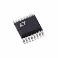
LTC3701EGN Linear Technology, LTC3701EGN Datasheet - Page 14

LTC3701EGN
Manufacturer Part Number
LTC3701EGN
Description
IC DC/DC CNTRLR STPDN DUAL16SSOP
Manufacturer
Linear Technology
Series
PolyPhase®r
Type
Step-Down (Buck)r
Datasheet
1.LTC3701EGN.pdf
(20 pages)
Specifications of LTC3701EGN
Internal Switch(s)
No
Synchronous Rectifier
No
Number Of Outputs
2
Voltage - Output
0.8 ~ 10 V
Current - Output
1A
Frequency - Switching
550kHz
Voltage - Input
2.5 ~ 10 V
Operating Temperature
-40°C ~ 85°C
Mounting Type
Surface Mount
Package / Case
16-SSOP
Lead Free Status / RoHS Status
Contains lead / RoHS non-compliant
Power - Output
-
Available stocks
Company
Part Number
Manufacturer
Quantity
Price
Part Number:
LTC3701EGN
Manufacturer:
LINEAR/凌特
Quantity:
20 000
Part Number:
LTC3701EGN#PBF
Manufacturer:
LT/凌特
Quantity:
20 000
Part Number:
LTC3701EGN#TR
Manufacturer:
LT/凌特
Quantity:
20 000
Part Number:
LTC3701EGN#TRPBF
Manufacturer:
LT/凌特
Quantity:
20 000
Company:
Part Number:
LTC3701EGNPBF
Manufacturer:
LINEAR
Quantity:
1 306
APPLICATIO S I FOR ATIO
LTC3701
internal oscillator frequency may be set by applying a DC
voltage to the PLLLPF pin. 550kHz operation can be
selected by floating the PLLLPF pin. The PLLLPF pin may
be connected to voltages as high as V
Efficiency Considerations
The efficiency of a switching regulator is equal to the
output power divided by the input power times 100%. It is
often useful to analyze individual losses to determine what
is limiting efficiency and which change would produce the
most improvement. Efficiency can be expressed as:
where L1, L2, etc. are the individual losses as a percentage
of input power.
Although all dissipative elements in the circuit produce
losses, five main sources usually account for most of the
losses in LTC3701 circuits: 1) LTC3701 DC bias current,
2) MOSFET gate charge current, 3) I
drop of the output diode and 5) transition losses.
1) The V
2) MOSFET gate charge current results from switching the
14
OSCILLATOR
EXTERNAL
Efficiency = 100% – (L1 + L2 + L3 + …)
the electrical characteristics, that excludes MOSFET
driver currents. V
increases with V
gate capacitance of the power MOSFET. Each time a
MOSFET gate is switched from low to high to low again,
a packet of charge dQ moves from PV
resulting dQ/dt is a current out of PV
IN
Figure 8. Phase-Locked Loop Block Diagram
(pin) current is the DC supply current, given in
EXTCLK/
MODE
IN
U
FREQUENCY
IN
DETECTOR
.
DIGITAL
PHASE/
current results in a small loss that
U
W
2
2.4V
R losses, 4) voltage
IN
IN
.
to ground. The
10k
PLLLPF
IN
R
LP
, which is
OSCILLATOR
U
3701 F08
C
LP
3) I
4) The output diode is a major source of power loss at high
5) Transition losses apply to the external MOSFET and
Other losses, including C
losses and inductor core losses, generally account for less
than 2% total additional loss.
Foldback Current Limiting
As described in the Output Diode Selection, the worst-
case diode dissipation occurs with a short-circuited out-
put when the diode conducts the current limit value almost
continuously. To prevent excessive heating in the diode,
foldback current limiting can be added to reduce the
current in proportion to the severity of the fault.
Foldback current limiting is implemented by adding di-
odes D
pin as shown in Figure 9. In a hard short (V
current will be reduced to approximately 50% of the
maximum output current.
typically much larger than the DC supply current. In
continuous mode, I
MOSFET, inductor and sense resistor. In continuous
mode, the average output current flows through L but
is “chopped” between the P-channel MOSFET in series
with R
plus R
with the resistance of L to obtain I
currents and is worse at high input voltages. The diode
loss is calculated by multiplying the forward voltage
times the load current times the diode duty cycle.
increase with higher operating frequencies and input
voltages. Transition losses can be estimated from:
Transition Loss = 2 (V
2
R losses are calculated from the DC resistances of the
FB1
SENSE
SENSE
and D
Figure 9. Foldback Current Limiting
and the output diode. The MOSFET R
multiplied by duty cycle can be summed
FB2
I
1/2 LTC3701
TH/RUN
between the output and the I
GATECHG
IN
V
FB
IN
)
2
I
O(MAX)
and C
= f • Q
R2
R1
+
C
OUT
2
P
RSS
R losses.
.
ESR dissipative
(f)
3701 F09
OUT
D
D
FB1
FB2
V
OUT
= 0V), the
TH
DS(ON)
/RUN
3701fa


