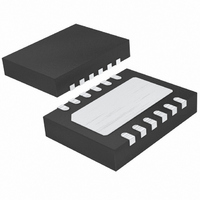
LTC3458EDE#PBF Linear Technology, LTC3458EDE#PBF Datasheet - Page 7

LTC3458EDE#PBF
Manufacturer Part Number
LTC3458EDE#PBF
Description
IC CONV DC/DC SYNC BOOST 12DFN
Manufacturer
Linear Technology
Type
Step-Up (Boost)r
Datasheet
1.LTC3458EDE.pdf
(16 pages)
Specifications of LTC3458EDE#PBF
Internal Switch(s)
Yes
Synchronous Rectifier
Yes
Number Of Outputs
1
Voltage - Output
2 ~ 7.5 V
Current - Output
1.4A
Frequency - Switching
1.5MHz
Voltage - Input
1.5 ~ 6 V
Operating Temperature
-40°C ~ 85°C
Mounting Type
Surface Mount
Package / Case
12-DFN
Dc To Dc Converter Type
Step Up
Pin Count
12
Input Voltage
6V
Output Voltage
2 to 7.5V
Switching Freq
1.15MHz
Output Current
1.6A
Efficiency
93%
Package Type
DFN EP
Output Type
Adjustable
Switching Regulator
Yes
Mounting
Surface Mount
Input Voltage (min)
1.5V
Operating Temp Range
-40C to 85C
Operating Temperature Classification
Industrial
Primary Input Voltage
6V
No. Of Outputs
1
No. Of Pins
12
Operating Temperature Range
-40°C To +85°C
Msl
MSL 1 - Unlimited
Rohs Compliant
Yes
Lead Free Status / RoHS Status
Lead free / RoHS Compliant
Power - Output
-
Lead Free Status / Rohs Status
Compliant
Available stocks
Company
Part Number
Manufacturer
Quantity
Price
PI FU CTIO S
SW (Pin 1): Switch Pin for Inductor Connection. During
discontinuous conduction mode an antiring resistor con-
nects SW to V
V
supply and decouple with 1μF minimum.
SYNC (Pin 3): Oscillator Synchronization Pin. A clock
pulse width of 100ns to 2μs is required to synchronize the
internal oscillator. This pin is disabled when grounded.
SHDN (Pin 4): Shutdown Pin. Grounding this pin shuts
down the IC. Connect to >1.25V to enable.
I
resistor from I
current according to the following formula:
where I
R
oscillator frequency, according to the formula:
where f
FB (Pin 7): Connect Resistor Divider Tap Here. The output
voltage can be adjusted from 2V to 7.5V. Feedback refer-
ence voltage is typically 1.23V.
COMP (Pin 8): g
pensation network is connected from this pin to ground to
compensate the loop. See the section “Compensating the
Feedback Loop” for guidelines.
LIM
IN
T
I
U
f
(Pin 6): Connect a resistor to ground to program the
LIMIT
OSC
(Pin 2): Input Supply Pin. Connect this to the input
(Pin 5): Adjustable Peak Current Limit. Connect a
LIMIT
OSC
=
=
U
0 2 0 004
is in MHz and R
R
.
200
is in amps and R
ILIM
IN
+
LIM
to reduce noise.
m
.
1
to GND to program the peak inductor
Error Amp Output. A frequency com-
U
•
R
T
T
is in kΩ.
ILIM
is in kΩ.
GND (Pin 9): Signal Ground Pin.
SS (Pin 10): Connect a capacitor between this pin and
ground to set soft-start period. 5μA of current is sourced
from SS during soft-start.
BURST (Pin 11): Burst Mode Threshold Adjust Pin. A
resistor/capacitor combination from this pin to ground
programs the average load current at which automatic
Burst Mode operation is entered, according to the formula:
where R
where C
To force fixed frequency PWM mode, connect BURST to
V
V
Internal Gate Drive Source for the Power Switches.
Exposed Pad (PGND) (Pin 13): Must be soldered to PCB
ground, for electrical contact and optimum thermal
performance.
OUT
OUT
t(msec) = C
R
C
V
OUT
BURST
BURST
through a 50k resistor.
(Pin 12): Output of the Synchronous Rectifier and
BURST(MIN)
BURST
=
1 23 1
=
=
.
I
C
BURST
SS
is in kΩ and I
⎛
⎜
⎝
OUT
10
10 000
(μF )• 200
+
,
and C
•
R
R
V
2
1
OUT
⎞
⎟
⎠
OUT
BURST
are in μF.
is in amps.
LTC3458
3458fa
7


