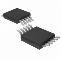
LTC1871IMS Linear Technology, LTC1871IMS Datasheet - Page 9

LTC1871IMS
Manufacturer Part Number
LTC1871IMS
Description
IC MULTI CONFIG SYNC ADJ 10MSOP
Manufacturer
Linear Technology
Type
Step-Up (Boost), Flyback, Sepicr
Datasheet
1.LTC1871EMS.pdf
(36 pages)
Specifications of LTC1871IMS
Internal Switch(s)
No
Synchronous Rectifier
No
Number Of Outputs
1
Voltage - Output
1.23 ~ 72 V
Current - Output
50mA
Frequency - Switching
50kHz ~ 1MHz
Voltage - Input
2.5 ~ 36 V
Operating Temperature
-40°C ~ 125°C
Mounting Type
Surface Mount
Package / Case
10-MSOP, Micro10™, 10-uMAX, 10-uSOP
Lead Free Status / RoHS Status
Contains lead / RoHS non-compliant
Power - Output
-
Available stocks
Company
Part Number
Manufacturer
Quantity
Price
Company:
Part Number:
LTC1871IMS
Manufacturer:
LT
Quantity:
10 000
Part Number:
LTC1871IMS
Manufacturer:
LINEAR
Quantity:
20 000
Company:
Part Number:
LTC1871IMS#3CFPBF
Manufacturer:
LT
Quantity:
2 043
Company:
Part Number:
LTC1871IMS#PBF
Manufacturer:
LT
Quantity:
2 058
Company:
Part Number:
LTC1871IMS-1
Manufacturer:
LT
Quantity:
10 000
Company:
Part Number:
LTC1871IMS-7
Manufacturer:
LT
Quantity:
10 000
OPERATION
The nominal operating frequency of the LTC1871 is pro-
grammed using a resistor from the FREQ pin to ground
and can be controlled over a 50kHz to 1000kHz range. In
addition, the internal oscillator can be synchronized to
an external clock applied to the MODE/SYNC pin and can
be locked to a frequency between 100% and 130% of its
nominal value. When the MODE/SYNC pin is left open, it
is pulled low by an internal 50k resistor and Burst Mode
operation is enabled. If this pin is taken above 2V or an
external clock is applied, Burst Mode operation is disabled
and the IC operates in continuous mode. With no load (or
an extremely light load), the controller will skip pulses in
order to maintain regulation and prevent excessive output
ripple.
The RUN pin controls whether the IC is enabled or is in a low
current shutdown state. A micropower 1.248V reference
and comparator C2 allow the user to program the supply
voltage at which the IC turns on and off (comparator C2
has 100mV of hysteresis for noise immunity). With the
RUN pin below 1.248V, the chip is off and the input supply
current is typically only 10μA.
An overvoltage comparator OV senses when the FB pin
exceeds the reference voltage by 6.5% and provides a
Figure 2. Using the SENSE Pin On the LTC1871
2b. SENSE Pin Connection for Precise
Control of Peak Current or for V
2a. SENSE Pin Connection for
Maximum Efficiency (V
GND
GND
V
V
IN
IN
GND
GND
V
V
SENSE
SENSE
IN
IN
GATE
GATE
L
L
V
V
R
SW
SW
SW
S
D
D
+
+
< 36V)
SW
V
C
V
C
1871 F02
OUT
OUT
OUT
OUT
> 36V
reset pulse to the main RS latch. Because this RS latch is
reset-dominant, the power MOSFET is actively held off for
the duration of an output overvoltage condition.
The LTC1871 can be used either by sensing the voltage
drop across the power MOSFET or by connecting the
SENSE pin to a conventional shunt resistor in the source
of the power MOSFET, as shown in Figure 2. Sensing the
voltage across the power MOSFET maximizes converter
effi ciency and minimizes the component count, but limits
the output voltage to the maximum rating for this pin (36V).
By connecting the SENSE pin to a resistor in the source
of the power MOSFET, the user is able to program output
voltages signifi cantly greater than 36V.
Programming the Operating Mode
For applications where maximizing the effi ciency at very
light loads (e.g., <100μA) is a high priority, the current
in the output divider could be decreased to a few micro-
amps and Burst Mode operation should be applied (i.e.,
the MODE/SYNC pin should be connected to ground).
In applications where fi xed frequency operation is more
critical than low current effi ciency, or where the lowest
output ripple is desired, pulse-skip mode operation should
be used and the MODE/SYNC pin should be connected
to the INTV
mode (DCM) operation down to near the limit defi ned
by the chip’s minimum on-time (about 175ns). Below
this output current level, the converter will begin to skip
cycles in order to maintain output regulation. Figures 3
and 4 show the light load switching waveforms for Burst
Mode and pulse-skip mode operation for the converter
in Figure 1.
Burst Mode Operation
Burst Mode operation is selected by leaving the MODE/
SYNC pin unconnected or by connecting it to ground. In
normal operation, the range on the I
no load to full load is 0.30V to 1.2V. In Burst Mode opera-
tion, if the error amplifi er EA drives the I
0.525V, the buffered I
C1 will be clamped at 0.525V (which corresponds to 25%
of maximum load current). The inductor current peak is
then held at approximately 30mV divided by the power
CC
pin. This allows discontinuous conduction
TH
input to the current comparator
TH
pin corresponding to
LTC1871
TH
voltage below
1871fe
9


