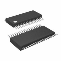
LTC3865EFE#TRPBF Linear Technology, LTC3865EFE#TRPBF Datasheet - Page 22

LTC3865EFE#TRPBF
Manufacturer Part Number
LTC3865EFE#TRPBF
Description
IC BUCK SYNC ADJ DUAL 38TSSOP
Manufacturer
Linear Technology
Type
Step-Down (Buck)r
Datasheet
1.LTC3865EUHPBF.pdf
(38 pages)
Specifications of LTC3865EFE#TRPBF
Internal Switch(s)
No
Synchronous Rectifier
Yes
Number Of Outputs
2
Voltage - Output
0.6 ~ 5 V
Frequency - Switching
250kHz ~ 770kHz
Voltage - Input
4.5 ~ 38 V
Operating Temperature
-40°C ~ 85°C
Mounting Type
Surface Mount
Package / Case
38-TSSOP Exposed Pad, 38-eTSSOP, 38-HTSSOP
Lead Free Status / RoHS Status
Lead free / RoHS Compliant
Current - Output
-
Power - Output
-
Available stocks
Company
Part Number
Manufacturer
Quantity
Price
LTC3865/LTC3865-1
APPLICATIONS INFORMATION
For applications where the main input power is below 5V,
tie the V
pins to the 5V input with a 1Ω or 2.2Ω resistor as shown
in Figure 8 to minimize the voltage drop caused by the
gate charge current. This will override the INTV
regulator and will prevent INTV
due to the dropout voltage. Make sure the INTV
is at or exceeds the R
which is typically 4.5V for logic-level devices.
Topside MOSFET Driver Supply (C
External bootstrap capacitors, C
pins supply the gate drive voltages for the topside MOSFETs.
Capacitor C
external diode D
When one of the topside MOSFETs is to be turned on, the
driver places the C
desired MOSFET. This enhances the MOSFET and turns on
the topside switch. The switch node voltage, SW, rises to
V
on, the boost voltage is above the input supply: V
= V
needs to be 100 times that of the total input capacitance
of the topside MOSFET(s). The reverse breakdown of the
external Schottky diode must be greater than V
When adjusting the gate drive level, the fi nal arbiter is the
total input current for the regulator. If a change is made
and the input current decreases, then the effi ciency has
improved. If there is no change in input current, then there
is no change in effi ciency.
22
IN
and the BOOST pin follows. With the topside MOSFET
IN
+ V
IN
INTVCC
and INTV
B
in the Functional Diagram is charged through
Figure 8. Setup for a 5V Input
. The value of the boost capacitor, C
LTC3865
B
from INTV
B
CC
voltage across the gate source of the
INTV
DS(ON)
pins together and tie the combined
V
CC
IN
test voltage for the MOSFET
CC
C
4.7μF
B
CC
INTVCC
R
when the SW pin is low.
, connected to the BOOST
1Ω
VIN
from dropping too low
B
+
, D
3865
B
C
5V
)
IN
F08
CC
CC
IN(MAX)
voltage
BOOST
linear
B
,
.
Undervoltage Lockout
The LTC3865/LTC3865-1 have two functions that help
protect the controller in case of undervoltage conditions.
A precision UVLO comparator constantly monitors the
INTV
voltage is present. It locks out the switching action when
INTV
a disturbance on the INTV
550mV of precision hysteresis.
Another way to detect an undervoltage condition is to
monitor the V
precision turn-on reference of 1.22V, one can use a resistor
divider to V
An extra 4.5μA of current fl ows out of the RUN pin once
the RUN pin voltage passes 1.22V. One can program the
hysteresis of the run comparator by adjusting the values
of the resistive divider. For accurate V
detection, V
C
The selection of C
ture and its impact on the worst-case RMS current drawn
through the input network (battery/fuse/capacitor). It can be
shown that the worst-case capacitor RMS current occurs
when only one controller is operating. The controller with
the highest (V
formula below to determine the maximum RMS capacitor
current requirement. Increasing the output current drawn
from the other controller will actually decrease the input
RMS ripple current from its maximum value. The out-of-
phase technique typically reduces the input capacitor’s RMS
ripple current by a factor of 30% to 70% when compared
to a single phase power supply solution.
In continuous mode, the source current of the top MOSFET
is a square wave of duty cycle (V
large voltage transients, a low ESR capacitor sized for the
IN
and C
CC
CC
is below 3.3V. To prevent oscillation when there is
voltage to ensure that an adequate gate-drive
OUT
IN
IN
to turn on the IC when V
Selection
OUT
IN
needs to be higher than 4.5V.
supply. Because the RUN pins have a
)(I
IN
is simplifi ed by the 2-phase architec-
OUT
) product needs to be used in the
CC
, the UVLO comparator has
OUT
)/(V
IN
IN
is high enough.
IN
undervoltage
). To prevent
3865fb


