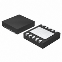
LTC3407EDD-3#TRPBF Linear Technology, LTC3407EDD-3#TRPBF Datasheet - Page 13

LTC3407EDD-3#TRPBF
Manufacturer Part Number
LTC3407EDD-3#TRPBF
Description
IC REG DC/DC DUAL STEPDOWN 10DFN
Manufacturer
Linear Technology
Type
Step-Down (Buck)r
Datasheet
1.LTC3407EDD-3PBF.pdf
(16 pages)
Specifications of LTC3407EDD-3#TRPBF
Internal Switch(s)
Yes
Synchronous Rectifier
Yes
Number Of Outputs
2
Voltage - Output
0.6 ~ 5 V
Current - Output
1A
Frequency - Switching
1.5MHz
Voltage - Input
2.5 ~ 5.5 V
Operating Temperature
-40°C ~ 85°C
Mounting Type
Surface Mount
Package / Case
10-DFN
Lead Free Status / RoHS Status
Lead free / RoHS Compliant
Power - Output
-
Available stocks
Company
Part Number
Manufacturer
Quantity
Price
APPLICATIONS INFORMATION
2. Are the C
C
3. The output feedback line should be routed away from
noisy components and traces, such as the SW line (Pins 4
and 7), and its trace should be minimized.
4. Keep sensitive components away from the SW pins.
The input capacitor C
SW traces and the inductors.
TYPICAL APPLICATIONS
OUT
returns current to GND and the (–) plate of C
OUT
and L1 closely connected? The (–) plate of
IN
should be routed away from the
800mA
V
V
5V
OUT2
3.3V
IN
10μF
Low Ripple Buck Regulators Using Ceramic Capacitors
C3
C1, C2, C3: TAIYO YUDEN JMK212BJ106MD-B
L1, L2: COILCRAFT LDO3310-222MX
*IF C1 IS GREATER THAN 3" FROM POWER SOURCE,
ADDITIONAL CAPACITANCE MAY BE REQUIRED.
100
C1*
10μF
95
90
85
60
55
50
80
75
70
65
2.2μH
10
L2
V
OUT
Effi ciency vs Load Current
= 3.3V
MODE/SYNC
SW2
V
IN
RUN2
OUT2
.
LOAD CURRENT (mA)
V
PULSE-SKIPPING MODE
NO LOAD ON OTHER CHANNEL
LTC3407-3
IN
GND
= 5V
V
IN
V
100
OUT
5. A ground plane is preferred, but if not available, keep
the signal and power grounds segregated with small signal
components returning to the GND pin at one point and
should not share the high current path of C
6. Flood all unused areas on all layers with copper. Flood-
ing with copper will reduce the temperature rise of power
components. These copper areas should be connected to
V
RUN1
= 1.8V
V
IN
SW1
POR
OUT1
or GND.
2.2μH
34073 TA02b
L1
R5
100k
1000
POWER-ON
RESET
34073 TA03a
C2
10μF
V
1.8V
800mA
OUT1
LTC3407-3
IN
or C
13
OUT
34073fb
.


