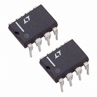
LT1507CN8 Linear Technology, LT1507CN8 Datasheet - Page 5

LT1507CN8
Manufacturer Part Number
LT1507CN8
Description
IC SW REG BUCK MODE ADJ 8-DIP
Manufacturer
Linear Technology
Type
Step-Down (Buck)r
Datasheet
1.LT1507CS8PBF.pdf
(20 pages)
Specifications of LT1507CN8
Internal Switch(s)
Yes
Synchronous Rectifier
No
Number Of Outputs
1
Voltage - Output
Adjustable
Current - Output
1.5A
Frequency - Switching
500kHz
Voltage - Input
4 ~ 15 V
Operating Temperature
0°C ~ 70°C
Mounting Type
Through Hole
Package / Case
8-DIP (0.300", 7.62mm)
Lead Free Status / RoHS Status
Contains lead / RoHS non-compliant
Power - Output
-
Available stocks
Company
Part Number
Manufacturer
Quantity
Price
Part Number:
LT1507CN8#PBF
Manufacturer:
LINEAR/凌特
Quantity:
20 000
PIN
BOOST (Pin 1): The BOOST pin is used to provide a drive
voltage, higher than the input voltage, to the internal
bipolar NPN power switch. Without this added voltage the
typical switch voltage loss would be about 1.5V. The
additional boost voltage allows the switch to saturate and
voltage loss approximates that of a 0.3 FET structure,
but with a much smaller die area. Efficiency improves from
TYPICAL PERFORMANCE CHARACTERISTICS
Kool M is a registered trademark of Magnetics, Incorporated.
Metglas is a registered trademark of AlliedSignal Incorporated.
2.5
2.0
1.5
1.0
0.5
12
10
U
8
6
4
2
0
0
*SEE "MORE THAN JUST VOLTAGE FEEDBACK"
Current Limit Foldback
0
0
Boost Pin Current
IN APPLICATIONS INFORMATION SECTION
FUNCTIONS
T
J
= 25 C
0.25
*POSSIBLE
UNDESIRED
STABLE POINT
FOR CURRENT
SOURCE LOAD
20
U
SWITCH CURRENT (A)
OUTPUT VOLTAGE (%)
0.50
40
U
FOLDBACK
CHARACTERISTICS
0.75
60
RESISTOR LOAD
CURRENT
SOURCE LOAD
MOS LOAD
1.00
W
80
LT1507 • TPC16
LT1507 • TPC13
U
1.25
100
0.001
1.50
1.25
1.00
0.75
0.50
0.25
0.01
1.0
0.1
0
CORE LOSS IS INDEPENDENT OF LOAD CURRENT
UNTIL LOAD CURRENT FALLS LOW ENOUGH
FOR CIRCUIT TO GO INTO DISCONTINUOUS MODE
4
Maximum Load Current
at V
Inductor Core Loss for 3.3V Output
1
PERMALLOY
V
V
I
OUT
OUT
IN
OUT
= 5V
= 1A
6
= 3.3V
Kool M
= 125
= 3.3V
INPUT VOLTAGE (V)
2
INDUCTANCE ( H)
®
8
TYPE 52 POWDERED IRON
Metglas
70% for conventional bipolar designs to greater than 85%
for these new parts.
V
with an input voltage between 4.5V and 15V. Under certain
conditions, input voltage may be reduced down to 4V.
Actual minimum operating voltage will always be higher
than the output voltage. It may be limited by switch
L = 2 H
IN
10
L = 3 H
®
L = 5 H
4
(Pin 2): Input Pin. The LT1507 is designed to operate
L = 10 H
V
OUT
12
6
LT1507 • TPC14
= 3.3V
LT1507 • TPC17
8
14
10
1.50
1.25
1.00
0.75
0.50
0.25
0.8
0.6
0.4
0.2
0
0
0
Switch Voltage Drop
0
Maximum Load Current
at V
T
J
OUT
= 25 C
0.25
3
= 5V
SWITCH CURRENT (A)
INPUT VOLTAGE (V)
0.50
6
0.75
L = 5 H
9
1.00
LT1507
L = 10 H
L = 20 H
12
1.25
LT1507 • TPC15
LT1507 • TPC18
5
1.50
15


