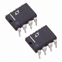
LT1507CN8-3.3 Linear Technology, LT1507CN8-3.3 Datasheet - Page 7

LT1507CN8-3.3
Manufacturer Part Number
LT1507CN8-3.3
Description
IC SW REG BUCK MODE 3.3V 8-DIP
Manufacturer
Linear Technology
Type
Step-Down (Buck)r
Datasheet
1.LT1507CS8PBF.pdf
(20 pages)
Specifications of LT1507CN8-3.3
Internal Switch(s)
Yes
Synchronous Rectifier
No
Number Of Outputs
1
Voltage - Output
3.3V
Current - Output
1.5A
Frequency - Switching
500kHz
Voltage - Input
4 ~ 15 V
Operating Temperature
0°C ~ 70°C
Mounting Type
Through Hole
Package / Case
8-DIP (0.300", 7.62mm)
Lead Free Status / RoHS Status
Contains lead / RoHS non-compliant
Power - Output
-
BLOCK
APPLICATIONS
Note: This application section is adapted from the more
complete version found in the LT1375/LT1376 data sheet.
If more details are desired consult the LT1375/LT1376
Applications Information section, but please acquaint
yourself thoroughly with this LT1507 information first so
that differences between the LT1375 and the LT1507 do
not cause confusion.
SHDN
SYNC
BIAS
V
IN
COMPARATOR
2
5
4
SHUTDOWN
DIAGRAM
REGULATOR
+
2.9V BIAS
2.38V
U
3.5 A
+
–
0.4V
–
INFORMATION
LOCKOUT
COMPARATOR
W
U
OSCILLATOR
SLOPE COMP
500kHz
INTERNAL
V
CC
W
+
0.1
U
8
Figure 1. Block Diagram
FOLDBACK
V
0.9V
–
CURRENT
C
–
+
CLAMP
LIMIT
CURRENT
SENSE
AMPLIFIER
VOLTAGE GAIN = 5
CURRENT
COMPARATOR
Q2
FEEDBACK PIN FUNCTIONS
The feedback pin (FB or SENSE) on the LT1507 is used to
set output voltage and also to provide several overload
protection features. The first part of this section deals with
selecting resistors to set output voltage and the remaining
part talks about foldback frequency and current limiting
created by the FB pin. Please read both parts before
S
R
g
SHIFT CIRCUIT
m
FREQUENCY
FLIP-FLOP
= 2000 mho
AMPLIFIER
R
S
ERROR
–
+
CIRCUITRY
DRIVER
2.42V
BOOST
1
3
7
6
LT1507 • BD
Q1
POWER
SWITCH
LT1507
V
GND
FB/SENSE
SW
7


