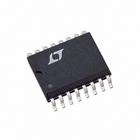
LTC1435CS Linear Technology, LTC1435CS Datasheet - Page 15

LTC1435CS
Manufacturer Part Number
LTC1435CS
Description
IC SW REG SYNC STEP-DOWN 16-SOIC
Manufacturer
Linear Technology
Type
Step-Down (Buck)r
Datasheet
1.LTC1435CGPBF.pdf
(20 pages)
Specifications of LTC1435CS
Internal Switch(s)
No
Synchronous Rectifier
Yes
Number Of Outputs
1
Voltage - Output
1.19 ~ 9 V
Current - Output
50mA
Frequency - Switching
125kHz
Voltage - Input
3.5 ~ 30 V
Operating Temperature
0°C ~ 70°C
Mounting Type
Surface Mount
Package / Case
16-SOIC (3.9mm Width)
Lead Free Status / RoHS Status
Contains lead / RoHS non-compliant
Power - Output
-
Available stocks
Company
Part Number
Manufacturer
Quantity
Price
Part Number:
LTC1435CS
Manufacturer:
LT/凌特
Quantity:
20 000
Part Number:
LTC1435CS#PBF
Manufacturer:
LINEAR/凌特
Quantity:
20 000
Part Number:
LTC1435CS8
Manufacturer:
LT/凌特
Quantity:
20 000
APPLICATIONS
Design Example
As a design example, assume V
22V(max), V
and C
Referring to Figure 3, a 10 H inductor falls within the
recommended range. To check the actual value of the
ripple current the following equation is used:
The highest value of the ripple current occurs at the
maximum input voltage:
The power dissipation on the topside MOSFET can be
easily estimated. Choosing a Siliconix Si4412DY results
in: R
voltage with T(estimated) = 50 C:
The most stringent requirement for the synchronous
N-channel MOSFET occurs when V
circuit). In this case the worst-case dissipation rises to:
With the 0.033 sense resistor I
increasing the Si4412DY dissipation to 950mW at a die
temperature of 105 C.
C
temperature. C
output ripple. The output ripple in continuous mode will be
IN
R
C
P
P
is chosen for an RMS current rating of at least 1.5A at
OSC
MAIN
SYNC
SENSE
DS(ON)
I
I
L
L
OSC
= 1.37(10
250
V
can immediately be calculated:
= 100mV/3A = 0.033
f L
2 5 22
OUT
3 3
= 0.042 , C
22
.
OUT
.
I
SC AVG
kHz
V
V
OUT
3 3
.
= 3.3V, I
1–
3 1
V
4
V
10
is chosen with an ESR of 0.03 for low
)/250 – 11 = 43pF
U
2
1 85
V
.
V
OUT
H
2
IN
RSS
3
MAX
1
INFORMATION
0 005 50
A
U
1
.
–
= 100pF. At maximum input
100
= 3A and f = 250kHz, R
3 3
22
R
.
IN
pF
DS ON
V
SC(AVG)
V
= 12V(nominal), V
W
C
250
OUT
1 1
25
kHz
. 2A
= 4A will result,
= 0 (i.e. short
C
U
0 042
122
.
mW
SENSE
IN
=
highest at the maximum input voltage. The output voltage
ripple due to ESR is approximately:
PC Board Layout Checklist
When laying out the printed circuit board, the following
checklist should be used to ensure proper operation of the
LTC1435. These items are also illustrated graphically in
the layout diagram of Figure 8. Check the following in your
layout:
1. Are the signal and power grounds segregated? The
2. Does the V
3. Are the SENSE
4. Does the (+) plate of C
5. Is the INTV
6. Keep the switching node SW away from sensitive small-
7. SGND should be exclusively used for grounding exter-
V
LTC1435 signal ground pin must return to the (–) plate
of C
the bottom N-channel MOSFET, anode of the Schottky
diode, and (–) plate of C
lead lengths as possible.
resistors? The resistive divider R1, R2 must be con-
nected between the (+) plate of C
The 100pF capacitor should be as close as possible to
the LTC1435.
minimum PC trace spacing? The filter capacitor be-
tween SENSE
possible to the LTC1435.
topside MOSFET(s) as closely as possible? This capaci-
tor provides the AC current to the MOSFET(s).
between INTV
pacitor carries the MOSFET driver peak currents.
signal nodes. Ideally the switch node should be placed
at the furthest point from the LTC1435.
nal components on C
ORIPPLE
OUT
. The power ground connects to the source of
= R
OSENSE
CC
ESR
CC
+
decoupling capacitor connected closely
–
and SENSE
( I
and SENSE
and the power ground pin? This ca-
pin connect directly to the feedback
L
) = 0.03 (1.112A) = 34mV
OSC
IN
IN
, I
, which should have as short
connect to the drain of the
TH
+
leads routed together with
–
, V
should be as close as
OUT
OSENSE
and signal ground.
LTC1435
and SFB pins.
15
P-P


