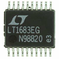
LT1738EG#TRPBF Linear Technology, LT1738EG#TRPBF Datasheet - Page 10

LT1738EG#TRPBF
Manufacturer Part Number
LT1738EG#TRPBF
Description
IC DC/DC CONTRLR LOW NOIS 20SSOP
Manufacturer
Linear Technology
Type
Step-Up (Boost), Cuk, Flybackr
Datasheet
1.LT1738EGPBF.pdf
(20 pages)
Specifications of LT1738EG#TRPBF
Internal Switch(s)
No
Synchronous Rectifier
No
Number Of Outputs
1
Voltage - Output
5 ~ 100 V
Frequency - Switching
20kHz ~ 250kHz
Voltage - Input
2.55 ~ 20 V
Operating Temperature
-40°C ~ 125°C
Mounting Type
Surface Mount
Package / Case
20-SSOP
Lead Free Status / RoHS Status
Lead free / RoHS Compliant
Current - Output
-
Power - Output
-
Available stocks
Company
Part Number
Manufacturer
Quantity
Price
OPERATIO
LT1738
The current slew feedback loop consists of the voltage
across the external sense resistor, which is internally
amplified and differentiated. The derivative is limited to a
value set by R
proportional to both the value of sense resistor and R
The two control loops are combined internally so that a
smooth transition from current slew control to voltage
slew control is obtained. When turning on, the driver
current will slew before voltage. When turning off, voltage
will slew before current. In general it is desirable to have
R
Internal Regulator
Most of the control circuitry operates from an internal 2.4V
low dropout regulator that is powered from V
internal low dropout design allows V
to 20V with stable operation of the controller. When SHDN
< 1.3V the internal regulator is completely disabled.
5V Regulator
A 5V regulator is provided for powering external circuitry.
This regulator draws current from V
be greater than 6.5V to be in regulation. It can sink or
source 10mA. The output is current limited to prevent
against destruction from accidental short circuits.
Safety and Protection Features
There are several safety and protection features on the
chip. The first is overcurrent limit. Normally the gate driver
will go low when the output of the internal sense amplifier
exceeds the voltage on the V
such that maximum output current is attained when the CS
pin voltage is 0.1V. At that level the outputs will be
immediately turned off (no slew). The effect of this control
is that the output voltage will foldback with overcurrent.
In addition, if the CS voltage exceeds 0.22V, the V
pins will be discharged to ground, resetting the soft-start
function. Thus if a short is present this will allow for faster
MOSFET turnoff and less MOSFET stress.
If the voltage on the FB pin exceeds regulation by approxi-
mately 0.22V, the outputs will immediately go low. The
implication is that there is an overvoltage fault.
10
VSL
and R
CSL
CSL
of similar value.
. The current slew rate is thus inversely
U
C
pin. The V
IN
IN
and requires V
to vary from 2.7V
C
pin is clamped
C
IN
and SS
. The
IN
CSL.
to
The voltage on GCL determines two features. The first is
the maximum gate drive voltage. This will protect the
MOSFET gate from overvoltage.
With GCL tied to a zener or an external voltage source then
the maximum gate driver voltage is approximately
V
voltage is determined by V
V
that prevents the gate driver pin from exceeding approxi-
mately 19V.
In addition, the GCL voltage determines undervoltage
lockout of the gate drive. This feature disables the gate
driver if V
on the MOSFET. This is helpful during start up to insure the
MOSFET has sufficient gate drive to saturate.
If GCL is tied to a voltage source or zener less than 6.8V,
the gate driver will not turn on until V
voltage by 0.8V. For V
insured to be off for V
V
If GCL is tied to V
(undervoltage lockout is disabled).
The gate drive has current limits for the drive currents. If
the sink or source current is greater than 300mA then the
current will be limited.
The V5 regulator also has internal current limiting that will
only guarantee 10mA output current.
There is also an on chip thermal shutdown circuit that will
turn off the output in the event the chip temperature rises
to dangerous levels. Thermal shutdown has hysteresis
that will cause a low frequency (<1kHz) oscillation to occur
as the chip heats up and cools down.
The chip has an undervoltage lockout feature that will
force the gate driver low in the event that V
2.5V. This insures predictable behavior during start up and
shut down. SHDN can be used in conjuction with an
external resistor divider to completely disable the part if
the input voltage is too low. This can be used to insure
adequate voltage to reliably run the converter. See the
section in Applications Information.
Table 1 summarizes these features.
GCL
IN
GCL
– 1.6V. There is an internal 19V zener on the GCL pin
– 0.2V. If GCL is tied to V
+ 0.8V.
IN
is too low to provide adequate voltage to turn
IN
IN
GCL
, the gate driver is always on
< 7.3V and it will be turned on by
above 6.5V, the gate drive is
IN
IN
, then the maximum gate
and is approximately
IN
IN
exceeds GCL
drops below
1738fa


