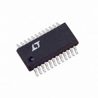
LTC3736EGN-2#PBF Linear Technology, LTC3736EGN-2#PBF Datasheet - Page 14

LTC3736EGN-2#PBF
Manufacturer Part Number
LTC3736EGN-2#PBF
Description
IC CTRLR SW SYNC DUAL 2PH 24SSOP
Manufacturer
Linear Technology
Series
PolyPhase®r
Type
Step-Down (Buck)r
Datasheet
1.LTC3736EGN-2PBF.pdf
(28 pages)
Specifications of LTC3736EGN-2#PBF
Internal Switch(s)
No
Synchronous Rectifier
Yes
Number Of Outputs
2
Voltage - Output
0.6 ~ 9.8 V
Current - Output
1A
Frequency - Switching
550kHz ~ 750kHz
Voltage - Input
2.75 ~ 9.8 V
Operating Temperature
-40°C ~ 85°C
Mounting Type
Surface Mount
Package / Case
24-SSOP
Lead Free Status / RoHS Status
Lead free / RoHS Compliant
Power - Output
-
Available stocks
Company
Part Number
Manufacturer
Quantity
Price
APPLICATIONS INFORMATION
LTC3736-2
The typical LTC3736-2 application circuit is shown in
Figure 13. External component selection for each of the
LTC3736-2’s controllers is driven by the load requirement
and begins with the selection of the inductor (L) and the
power MOSFETs (MP and MN).
Power MOSFET Selection
Each of the LTC3736-2’s two controllers requires two
external power MOSFETs: a P-channel MOSFET for the
topside (main) switch and an N-channel MOSFET for the
bottom (synchronous) switch. Important parameters for
the power MOSFETs are the breakdown voltage V
threshold voltage V
transfer capacitance C
total gate charge Q
The gate drive voltage is the input supply voltage. Since
the LTC3736-2 is designed for operation down to low input
voltages, a sublogic level MOSFET (R
V
this voltage. When these MOSFETs are used, make sure that
the input supply to the LTC3736-2 is less than the absolute
maximum MOSFET V
The P-channel MOSFET’s on-resistance is chosen based on
the required load current. The maximum average output
load current I
rent minus half the peak-to-peak ripple current I
The LTC3736-2’s current comparator monitors the drain-
to-source voltage V
is sensed between the SENSE
inductor current is limited by the current threshold, set by
the voltage on the I
voltage on the I
the maximum current sense threshold ΔV
approximately 240mV when IPRG is fl oating (167mV when
IPRG is tied low; 345mV when IPRG is tied high).
The output current that the LTC3736-2 can provide is
given by:
14
GS
I
OUT MAX
= 2.5V) is required for applications that work close to
(
)
OUT(MAX)
=
TH
Δ
V
pin is internally clamped, which limits
GS(TH)
G
TH
SENSE MAX
R
DS
.
DS ON
GS
pin of the current comparator. The
RSS
is equal to the peak inductor cur-
of the P-channel MOSFET, which
(
rating, which is typically 8V.
, on-resistance R
(
, turn-off delay t
)
)
+
–
and SW pins. The peak
I
RIPPLE
DS(ON)
2
DS(ON)
D(OFF)
SENSE(MAX)
guaranteed at
, reverse
BR(DSS)
and the
RIPPLE
to
,
.
A reasonable starting point is setting ripple current I
to be 40% of I
yields:
or Duty Cycle < 20%.
However, for operation above 20% duty cycle, slope
compensation has to be taken into consideration to select
the appropriate value of R
amount of load current:
where SF is a scale factor whose value is obtained from
the curve in Figure 1.
These must be further derated to take into account the
signifi cant variation in on-resistance with temperature.
The following equation is a good guide for determin-ing
the required R
tion), allowing some margin for variations in the LTC3736-2
and external component values:
The
perature variation in on-resistance, which is typically
about 0.4% / °C, as shown in Figure 4. Junction-to-case
temperature T
a maximum ambient temperature of 70°C, using
1.3 in the above equation is a reasonable choice.
The power dissipated in the top and bottom MOSFETs
strongly depends on their respective duty cycles and load
current. When the LTC3736-2 is operating in continuous
mode, the duty cycles for the MOSFETs are:
R
R
R
Bottom N C
Top P Channel Duty Cycle
DS ON MAX
DS ON MAX
DS ON MAX
ρ
T
(
(
(
is a normalizing term accounting for the tem-
-
)(
)(
)(
DS(ON)MAX
-
JC
OUT(MAX)
)
)
)
h h annel Duty Cycle
is about 10°C in most applications. For
=
=
=
5
6
5
6
5
6
•
•
• . •
. Rearranging the above equation
SF
0 9
Δ
at 25°C (manufacturer’s specifi ca-
V
I
DS(ON)
OUT MAX
SENSE MAX
•
Δ
SF
V
(
I
OUT MAX
SENSE MAX
•
(
to provide the required
I
Δ
OUT MAX
=
(
)
V
V
SENSE MAX
(
)
V
(
OUT
=
IN
)
V
IN
)
(
) )
• ρ
–
V
IN
V
T
)
OUT
ρ
RIPPLE
80°C
37362fb
~


