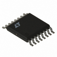
LT1940EFE#TR Linear Technology, LT1940EFE#TR Datasheet - Page 5

LT1940EFE#TR
Manufacturer Part Number
LT1940EFE#TR
Description
IC REG SW DUAL 1.4A STDN 16TSSOP
Manufacturer
Linear Technology
Type
Step-Down (Buck)r
Datasheet
1.LT1940EFEPBF.pdf
(20 pages)
Specifications of LT1940EFE#TR
Internal Switch(s)
Yes
Synchronous Rectifier
No
Number Of Outputs
2
Voltage - Output
1.25 ~ 22 V
Current - Output
1.4A
Frequency - Switching
1.1MHz
Voltage - Input
3.6 ~ 25 V
Operating Temperature
-40°C ~ 85°C
Mounting Type
Surface Mount
Package / Case
16-TSSOP Exposed Pad, 16-eTSSOP, 16-HTSSOP
Lead Free Status / RoHS Status
Contains lead / RoHS non-compliant
Power - Output
-
Available stocks
Company
Part Number
Manufacturer
Quantity
Price
PI FU CTIO S
TYPICAL PERFOR A CE CHARACTERISTICS
BOOST1, BOOST2 (Pins 1, 8): The BOOST pins are used
to provide drive voltages, higher than the input voltage, to
the internal bipolar NPN power switches.Tie through a
diode from V
SW1, SW2 (Pins 2, 7): The SW pins are the outputs of the
internal power switches. Connect these pins to the induc-
tors, catch diodes and boost capacitors.
V
LT1940’s internal regulator and to the internal power
switches. These pins must be tied to the same source, and
must be locally bypassed.
FB1, FB2 (Pins 9, 16): The LT1940 regulates each feed-
back pin to 1.25V. Connect the feedback resistor divider
taps to these pins.
V
internal error amps. The voltages on these pins control the
peak switch currents. These pins are normally used to
compensate the control loops, but can also be used to
override the loops. Pull these pins to ground with an open
drain to shut down each switching regulator.
IN
C1
1.4
1.2
1.0
0.8
0.6
0.4
0.2
U
, V
(Pins 3, 4, 5, 6): The V
0
–50
RUN/SS Thresholds vs
Temperature
C2
–25
(Pins 10, 15): The V
U
OUT
0
TEMPERATURE ( C)
TO RUN
25
or from V
U
TO SWITCH
50
75
IN
W
IN
.
C
100
pins supply current to the
pins are the outputs of the
1940 G13
U
125
6.0
5.5
5.0
4.5
4.0
3.5
3.0
Minimum Input Voltage,
V
1
V
OUT
V
IN
IN
TO START
TO RUN
= 3.3V
LOAD CURRENT (mA)
10
BOOST DIODE
TIED TO OUTPUT
BOOST DIODE
TIED TO INPUT
PG1, PG2 (Pins 11, 14): The Power Good pins are the
open collector outputs of an internal comparator. PG
remains low until the FB pin is within 10% of the final
regulation voltage. As well as indicating output regulation,
the PG pins can be used to sequence the two switching
regulators. These pins can be left unconnected. The PG
outputs are valid when V
of the RUN/SS pins is high. The PG comparators are
disabled in shutdown.
RUN/SS1, RUN/SS2 (Pins 12, 13): The RUN/SS pins are
use to shut down the individual switching regulators and
the internal bias circuits. They also provide a soft-start
function. To shut down either regulator, pull the RUN/SS
pin to ground with an open drain or collector. Tie a
capacitor from these pins to ground to limit switch current
during start-up. If neither feature is used, leave these pins
unconnected.
GND (Pin 17): The Exposed Pad of the package provides
both electrical contact to ground and good thermal con-
tact to the printed circuit board. The Exposed Pad must be
soldered to the circuit board for proper operation.
T
D
100
A
BOOST
= 25 C
= BAT54
1940 G14
1000
7.5
7.0
6.5
6.0
5.5
5.0
4.5
IN
LT1940/LT1940L
Minimum Input Voltage,
V
1
is greater than 2.4V and either
V
V
OUT
IN
IN
TO START
TO RUN
= 5V
LOAD CURRENT (mA)
10
BOOST DIODE
TIED TO OUTPUT
BOOST DIODE
TIED TO INPUT
100
T
D
A
BOOST
= 25 C
= BAT54
1940 G14
1940fa
5
1000


