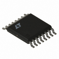
LT3433IFE#TR Linear Technology, LT3433IFE#TR Datasheet - Page 3

LT3433IFE#TR
Manufacturer Part Number
LT3433IFE#TR
Description
IC CONV DC/DC 200KHZ SW 16-TSSOP
Manufacturer
Linear Technology
Type
Step-Down (Buck), Step-Up (Boost)r
Datasheet
1.LT3433EFEPBF.pdf
(16 pages)
Specifications of LT3433IFE#TR
Internal Switch(s)
Yes
Synchronous Rectifier
No
Number Of Outputs
1
Voltage - Output
3.3 ~ 20 V
Current - Output
500mA
Frequency - Switching
200kHz
Voltage - Input
4 ~ 60 V
Operating Temperature
-40°C ~ 125°C
Mounting Type
Surface Mount
Package / Case
16-TSSOP Exposed Pad, 16-eTSSOP, 16-HTSSOP
Lead Free Status / RoHS Status
Contains lead / RoHS non-compliant
Power - Output
-
Available stocks
Company
Part Number
Manufacturer
Quantity
Price
ELECTRICAL CHARACTERISTICS
SYMBOL
V
I
g
A
I
f
V
I
t
t
Note 1: Absolute Maximum Ratings are those values beyond which the life
of a device may be impaired.
Note 2: Supply current specification does not include switch drive
currents. Actual supply currents will be higher.
Note 3: “Normal Operation” supply current specification does not include
I
current.
Note 4: Minimum times are tested using the high side switch with a 35
load to ground.
TYPICAL PERFOR A CE CHARACTERISTICS
The
V
FB
SW
O
BURST_EN
ON(MIN)
OFF(MIN)
BIAS
m
FB
V
BURST_EN
V
IN
500
100
FB
400
300
200
/V
= 13.8V, V
0
currents. Powering the V
VC
0
Maximum Output Current
vs V
denotes specifications that apply over the full operating temperature range, otherwise specifications are at T
BRIDGED
IN
10
PARAMETER
Feedback Reference Voltage
Feedback Reference Line Regulation
V
Error Amplifier Transconductance
Error Amplifier Voltage Gain
Control Voltage to Switch Transconductance
Operating Frequency
Foldback Frequency
Burst Enable Threshold
Input Bias Current
Minimum Switch On Time
Minimum Switch Off Time
FB
BUCK
FB
20
= 1.25V, V
Pin Input Bias Current
SEE TYPICAL APPLICATION
ON THE FIRST PAGE OF
THIS DATA SHEET
V
IN
30
(V)
BIAS
OUT
40
pin externally reduces I
= 5V, V
W
V
T
A
OUT
50
= 25 C
= 5V
3433 G11
U
BURST_EN
60
= 0V, V
2.4
2.8
2.6
2.2
CC
–50
supply
V
vs Temperature
BIAS
BST
CONDITIONS
5.5V V
V
V
V
R
R
FB
FB
BURST_EN
L
L
= 35 (Note 4)
= 35 (Note 4)
Output Voltage
– V
> 1V
= 0V
IN
0
TEMPERATURE ( C)
IN
= 5V, unless otherwise noted.
60V
2V
Note 5: This IC includes overtemperature protection that is intended to
protect the device during momentary overload conditions. Junction
temperature will exceed 125 C when overtemperature protection is active.
Continuous operation above the specified maximum operating junction
temperature may impair device reliability.
Note 6: The LT3433E is guaranteed to meet performance specifications
from 0 C to 125 C junction temperature. Specifications over the – 40 C to
125 C operating junction temperature range are assured by design,
characterization and correlation with statistical process controls. The
LT3433I is guaranteed over the full –40 C to 125 C operating junction
temperature range.
50
100
3433 G01
125
620
590
560
530
500
0
V
vs V
IN
T
1.224
1.215
A
MIN
200
185
170
= 25 C
Supply Current
IN
Supply Voltage
15
1.231
0.002
TYP
270
200
250
500
0.6
0.8
35
66
50
35
V
IN
A
30
(V)
= 25 C.
LT3433
1.238
1.245
MAX
0.01
100
330
215
230
450
800
45
umhos
UNITS
3433 G02
3
3433f
%/V
kHz
kHz
kHz
A/V
nA
dB
ns
ns
60
V
V
V
A


