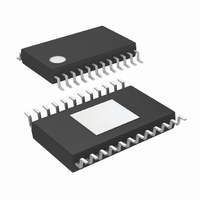
LTC3862IFE#PBF Linear Technology, LTC3862IFE#PBF Datasheet - Page 12

LTC3862IFE#PBF
Manufacturer Part Number
LTC3862IFE#PBF
Description
IC CTRLR DC/DC MULTI-PH 24TSSOP
Manufacturer
Linear Technology
Type
Step-Up (Boost)r
Datasheet
1.LTC3862EGNPBF.pdf
(40 pages)
Specifications of LTC3862IFE#PBF
Internal Switch(s)
No
Synchronous Rectifier
No
Number Of Outputs
1
Voltage - Output
1.22 ~ 200 V
Current - Output
50mA
Frequency - Switching
300kHz
Voltage - Input
4 ~ 36 V
Operating Temperature
-40°C ~ 125°C
Mounting Type
Surface Mount
Package / Case
24-TSSOP Exposed Pad, 24-eTSSOP, 24-HTSSOP
Lead Free Status / RoHS Status
Lead free / RoHS Compliant
Power - Output
-
Available stocks
Company
Part Number
Manufacturer
Quantity
Price
LTC3862
The Control Loop
The LTC3862 uses a constant frequency, peak current
mode step-up architecture with its two channels operat-
ing 180 degrees out of phase. During normal operation,
each external MOSFET is turned on when the clock for
that channel sets the PWM latch, and is turned off when
the main current comparator, ICMP , resets the latch. The
peak inductor current at which ICMP trips and resets the
latch is controlled by the voltage on the ITH pin, which is
the output of the error amplifi er, EA. The error amplifi er
compares the output feedback signal at the V
internal 1.223V reference and generates an error signal
at the ITH pin. When the load current increases it causes
a slight decrease in V
which causes the EA to increase the ITH voltage until the
average inductor current matches the new load current.
After the MOSFET is turned off, the inductor current fl ows
through the boost diode into the output capacitor and load,
until the beginning of the next clock cycle.
Cascaded LDOs Supply Power to the Gate Driver and
Control Circuitry
The LTC3862 contains two cascaded PMOS output stage
low dropout voltage regulators (LDOs), one for the gate
OPERATION
12
LTC3862
FB
relative to the reference voltage,
1.223V
R2
Figure 1. Cascaded LDOs Provide Gate Drive and Control Circuitry Power
NOTE: PLACE C
–
R1
+
SGND
1.223V
R4
VCC
–
R3
+
FB
AND C
pin to the
SGND
3V8
CAPACITORS AS CLOSE AS POSSIBLE TO DEVICE PINS
INTV
P-CH
CC
CIRCUITS
ANALOG
drive supply (INTV
and digital control circuitry (3V8). A block diagram of this
power supply arrangement is shown in Figure 1.
The Gate Driver Supply LDO (INTV
The 5V output (INTV
V
ers. The INTV
minimum of 4.7μF of ceramic capacitance (X5R or better),
placed as close as possible to the IC pins. If two power
MOSFETs are connected in parallel for each channel in
order to increase the output power level, or if a single
MOSFET with a Q
recommended that the bypass capacitance be increased
to a minimum of 10μF .
An undervoltage lockout (UVLO) circuit senses the INTV
regulator output in order to protect the power MOSFETs
from operating with inadequate gate drive. For the LTC3862
the rising UVLO threshold is typically 3.3V and the hyster-
esis is typically 400mV. The LTC3862 was optimized for
logic-level power MOSFETs and applications where the
output voltage is less than 50V to 60V. For applications
requiring standard threshold power MOSFETs, please refer
to the LTC3862-1 data sheet.
3V8
IN
P-CH
and supplies power to the power MOSFET gate driv-
LOGIC
CC
pin should be bypassed to PGND with a
G
CC
INTV
greater than 50nC is used, then it is
PGND
SGND
CC
GATE
) and one for the low voltage analog
3V8
V
CC
IN
) of the fi rst LDO is powered from
3862 F01
C
C
C
IN
VCC
3V8
CC
)
3862fb
CC


