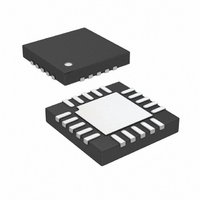
LTC3603IUF#PBF Linear Technology, LTC3603IUF#PBF Datasheet

LTC3603IUF#PBF
Specifications of LTC3603IUF#PBF
Available stocks
Related parts for LTC3603IUF#PBF
LTC3603IUF#PBF Summary of contents
Page 1
... L, LT, LTC, LTM, Burst Mode, OPTI-LOOP , Linear Technology and the Linear logo are registered trademarks and ThinSOT is a trademark of Linear Technology Corporation. All other trademarks are the property of their respective owners. Protected by U.S. Patents including 5481178, 6580258, 6498466, 6611131, 6177787, 5705919, 5847554. Effi ...
Page 2
... LTC3603IMSE #PBF LTC3603IMSE#TRPBF LTC3603EUF#PBF LTC3603EUF#TRPBF LTC3603IUF#PBF LTC3603IUF#TRPBF Consult LTC Marketing for parts specifi ed with wider operating temperature ranges. *The temperature grade is identifi label on the shipping container. Consult LTC Marketing for information on non-standard lead based fi nish parts. For more information on lead free part marking, go to: For more information on tape and reel specifi ...
Page 3
ELECTRICAL CHARACTERISTICS junction temperature range, otherwise specifi cations are at T SYMBOL PARAMETER PV Operating Voltage Range IN V Regulated Feedback Voltage FB ∆V Feedback Voltage Line Regulation FB(LINEREG) ∆V Feedback Voltage Load Regulation FB(LOADREG) ∆V Power Good Range PGOOD ...
Page 4
LTC3603 TYPICAL PERFORMANCE CHARACTERISTICS Burst Mode Operation OUTPUT VOLTAGE 50mV/DIV INDUCTOR CURRENT 500mA/DIV V = 12V 10μs/DIV 3.3V OUT LOAD = 50mA V vs Temperature REF 0.6006 V = 12V IN 0.6004 0.6002 0.6000 0.5998 0.5996 0.5994 ...
Page 5
TYPICAL PERFORMANCE CHARACTERISTICS Frequency vs Temperature 1020 R = 105kΩ OSC 1015 1010 1005 1000 995 990 985 980 50 100 –50 – TEMPERATURE (°C) 3603 G09 Minimum Peak Inductor Current vs Burst Clamp Voltage 3.0 2.5 ...
Page 6
LTC3603 TYPICAL PERFORMANCE CHARACTERISTICS Load Regulation 0.10 FIGURE 6 CIRCUIT V = 12V IN 0 –0.10 –0.20 0 0.5 1 1.5 2 2.5 LOAD CURRENT (A) 3603 G18 PIN FUNCTIONS MSE/UF Package INTV (Pin 1/Pin 3): Output of Internal 5V ...
Page 7
BLOCK DIAGRAM 1.2μA 0.6V VOLTAGE REFERENCE TRACK/SS 1ms SOFT-START ERROR AMPLIFIER + + + V FB – SYNC/MODE + 0.54V – + – 0.66V PGOOD ITH SLOPE COMPENSATION RECOVERY BCLAMP BURST MAIN COMPARATOR + I-COMPARATOR – + – SLOPE COMPENSATION ...
Page 8
LTC3603 OPERATION Main Control Loop The LTC3603 is a monolithic, constant-frequency, current mode step-down DC/DC converter. During normal operation, the internal top power switch (N-channel MOSFET) is turned on at the beginning of each clock cycle. Current in the inductor ...
Page 9
OPERATION resistor should be chosen to correspond to a frequency that is 25% lower than the synchronization frequency. When synchronized, the LTC3603 will operate in pulse- skipping mode. Dropout Operation When the input supply voltage decreases toward the output voltage, ...
Page 10
LTC3603 APPLICATIONS INFORMATION The basic LTC3603 application circuit is shown on the front page of this data sheet. External component selection is determined by the maximum load current and begins with the selection of the inductor value and operating frequency ...
Page 11
APPLICATIONS INFORMATION characteristics. The choice of which style inductor to use mainly depends on the price vs size requirements and any radiated fi eld/EMI requirements. New designs for surface mount inductors are available from Coiltronics, Coilcraft, Toko and Sumida. C ...
Page 12
LTC3603 APPLICATIONS INFORMATION Burst Clamp Programming If the voltage on the SYNC/MODE pin is in the range of 0.42V to 1V, Burst Mode operation is enabled. During Burst Mode operation, the voltage on the SYNC/MODE pin determines the burst clamp ...
Page 13
APPLICATIONS INFORMATION the BOOST pin rises INTV IN CC MOSFET fully enhanced. For most applications, a 0.22μF ceramic capacitor is appropriate for C D should have a reverse breakdown voltage that is BST greater than PV . ...
Page 14
LTC3603 APPLICATIONS INFORMATION TIME Figure 5b. Ratiometric Tracking TIME Figure 5c. Coincident Tracking Effi ciency Considerations The effi ciency of a switching regulator is equal to the output power divided by the input power times 100 often useful ...
Page 15
APPLICATIONS INFORMATION To prevent the LTC3603 from exceeding the maximum junction temperature, the user will need to do some thermal analysis. The goal of the thermal analysis is to determine whether the power dissipated exceeds the maximum junction temperature of ...
Page 16
LTC3603 APPLICATIONS INFORMATION R PG 200k PGOOD R OSC 105k C ITH R ITH 1nF 4.32k R1 105k R2 475k L1: VISHAY IHLP2525CZER2R2MO1 C : TAIYO YUDEN TMK325BJ226MM TDK C3225X5ROJ107M OUT Figure 6. 12V to 3.3V, 2.5A ...
Page 17
TYPICAL APPLICATIONS 845k 200k PGOOD R4 R OSC 137k 105k C ITH R ITH 1nF 4.32k R1 105k 10pF 210k L1: VISHAY IHLP2525CZER1R0MO1 C : TAIYO YUDEN TMK325BJ226MM TAIYO YUDEN AMK316BJ107ML ...
Page 18
LTC3603 TYPICAL APPLICATIONS Effi ciency vs Load Current, 1.8V Regulator at 1MHz, Burst Mode Operation 100 7. 12V 0.001 0.01 0.1 LOAD CURRENT (A) 3.3V, 2.5A ...
Page 19
PACKAGE DESCRIPTION 2.845 ± 0.102 (.112 ± .004) 5.23 (.206) MIN 0.305 ± 0.038 (.0120 ± .0015) TYP RECOMMENDED SOLDER PAD LAYOUT DETAIL “A” 0.254 (.010) GAUGE PLANE DETAIL “A” 0.18 (.007) NOTE: 1. DIMENSIONS IN MILLIMETER/(INCH) 2. DRAWING NOT ...
Page 20
LTC3603 PACKAGE DESCRIPTION 4.50 0.05 3.10 0.05 2.45 0.05 2.00 REF 2.45 0.05 RECOMMENDED SOLDER PAD PITCH AND DIMENSIONS APPLY SOLDER MASK TO AREAS THAT ARE NOT SOLDERED 4.00 0.10 PIN 1 TOP MARK (NOTE 6) 4.00 0.10 NOTE: 1. ...
Page 21
... Added Typical Application to back page Information furnished by Linear Technology Corporation is believed to be accurate and reliable. However, no responsibility is assumed for its use. Linear Technology Corporation makes no representa- tion that the interconnection of its circuits as described herein will not infringe on existing patent rights. LTC3603 ...
Page 22
... Q SD 95% Effi ciency 24V 0.6V, IN OUT(MIN) < 15μA, 9mm × 9mm QFN64 I = 900μ 95% Effi ciency 32V 0.6V, IN OUT(MIN) < 15μA, 9mm × 9mm QFN64 I = 900μ 0211 REV B • PRINTED IN USA © LINEAR TECHNOLOGY CORPORATION 2009 /2, REF 3603fb ...


