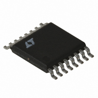
LT1956IFE#PBF Linear Technology, LT1956IFE#PBF Datasheet - Page 19

LT1956IFE#PBF
Manufacturer Part Number
LT1956IFE#PBF
Description
IC REG SW 1.5A HV STPDWN 16TSSOP
Manufacturer
Linear Technology
Type
Step-Down (Buck)r
Datasheet
1.LT1956EGNPBF.pdf
(28 pages)
Specifications of LT1956IFE#PBF
Internal Switch(s)
Yes
Synchronous Rectifier
No
Number Of Outputs
1
Voltage - Output
1.2 ~ 45 V
Current - Output
1.5A
Frequency - Switching
500kHz
Voltage - Input
5.5 ~ 60 V
Operating Temperature
-40°C ~ 125°C
Mounting Type
Surface Mount
Package / Case
16-TSSOP Exposed Pad, 16-eTSSOP, 16-HTSSOP
Dc To Dc Converter Type
Step Down
Pin Count
16
Input Voltage
60V
Output Voltage
1.2 to 45V
Switching Freq
540KHz
Output Current
3A
Package Type
TSSOP EP
Output Type
Adjustable
Switching Regulator
Yes
Line Regulation
0.15%/V
Mounting
Surface Mount
Input Voltage (min)
5.5V
Operating Temperature Classification
Automotive
Lead Free Status / RoHS Status
Lead free / RoHS Compliant
Power - Output
-
Lead Free Status / Rohs Status
Compliant
Available stocks
Company
Part Number
Manufacturer
Quantity
Price
APPLICATIO S I FOR ATIO
Boost current loss:
Quiescent current loss:
Example: with V
Total power dissipation in the IC is given by:
Thermal resistance for the LT1956 packages is influenced
by the presence of internal or backside planes.
SSOP (GN16) Package: With a full plane under the GN16
package, thermal resistance will be about 85 C/W.
TSSOP (Exposed Pad) Package: With a full plane under the
TSSOP package, thermal resistance (
45 C/W.
To calculate die temperature, use the proper thermal
resistance (
worst-case ambient temperature:
When estimating ambient, remember the nearby catch
diode and inductor will also be dissipating power.
P
P
P
SW
Q
BOOST
R
t
t
t
t
f = switch frequency
P
T
P
P
EFF
r
f
Ir
J
BOOST
Q
TOT
SW
= (V
= (V
= t
12 0 0015
= T
= effective switch current/voltage overlap time
= (t
0 125 0 171 0 296
= switch resistance ( 0.3) hot
If
= 0.296W + 0.058W + 0.033W = 0.39W
= P
V
0 3 1 5
.
A
IN
IN
IN
= (I
.
r
.
+ (
/1.7)ns
/1.2)ns
5
SW
+ t
12
0 0015
JA
V
OUT
2
.
OUT
f
JA
12
+ P
) number for the desired package an add in
2
+ t
1 36
IN
/0.05)ns
.
/
• P
2
Ir
BOOST
= 12V, V
U
V
5 0 003
I
+ t
TOT
OUT
IN
If
57 10
V
.
)
)
OUT
0 058
/
+ P
36
.
U
•
.
OUT
Q
0 003
W
W
.
9
= 5V and I
0 033
.
1 2 1 12 500 10
W
/
W
JA
OUT
) will be about
= 1A:
U
•
3
Notice that the catch diode’s forward voltage contributes
a significant loss in the overall system efficiency. A larger,
low V
Typical thermal resistance of the board is 10 C/W. Taking
the catch diode and inductor power dissipation into ac-
count and using the example calculations for LT1956 dis-
sipation, the LT1956 die temperature will be estimated as:
With the GN16 package (
temperature of 70 C:
With the TSSOP package (
temperature of 70 C:
Die temperature can peak for certain combinations of
V
switch AC losses, quiescent and catch diode losses, a
lower V
losses. In general, the maximum and minimum V
should be checked with maximum typical load current for
calculation of the LT1956 die temperature. If a more
accurate die temperature is required, a measurement of
the SYNC pin resistance (to GND) can be used. The SYNC
pin resistance can be measured by forcing a voltage no
greater than 0.5V at the pin and monitoring the pin
current over temperature in a oven. This should be done
with minimal device power (low V
[V
ambient (oven) temperature.
IN
C
V
P
L
P
T
T
T
P
P
, V
DCR
J
J
J
= 0V]) in order to calibrate SYNC pin resistance with
DIODE
F
DIODE
INDUCTOR
INDUCTOR
F
= T
= 70 + (85 • 0.39) + (10 • 0.47) = 108 C
= 70 + (45 • 0.37) + (10 • 0.47) = 91 C
= Forward voltage of diode (assume 0.63V at 1A)
OUT
diode can improve efficiency by several percent.
IN
= inductor DC resistance (assume 0.1 )
A
and load current. While higher V
+ (
may generate greater losses due to switch DC
( )(
( . )(
0 63 12 5 1
V V
= (I
= (1)(0.1) = 0.1W
JA
F
LOAD
• P
IN
12
TOT
–
)(L
V
– )( )
) + (10 • [P
V
IN
DCR
OUT
LT1956/LT1956-5
JA
JA
)
)(
= 85 C/W), at an ambient
I
LOAD
= 45 C/W) at an ambient
0 37
.
DIODE
IN
)
W
and no switching
+ P
IN
gives greater
INDUCTOR
IN
19
levels
])
1956f


