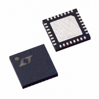
LTC3731CUH Linear Technology, LTC3731CUH Datasheet - Page 21

LTC3731CUH
Manufacturer Part Number
LTC3731CUH
Description
IC SW REG CTRLR SYNC BUCK 32QFN
Manufacturer
Linear Technology
Series
PolyPhase®r
Type
Step-Down (Buck)r
Datasheet
1.LTC3731CUHPBF.pdf
(32 pages)
Specifications of LTC3731CUH
Internal Switch(s)
No
Synchronous Rectifier
Yes
Number Of Outputs
1
Voltage - Output
0.6 ~ 6 V
Frequency - Switching
225kHz ~ 680kHz
Voltage - Input
4 ~ 36 V
Operating Temperature
0°C ~ 70°C
Mounting Type
Surface Mount
Package / Case
32-QFN
Lead Free Status / RoHS Status
Contains lead / RoHS non-compliant
Current - Output
-
Power - Output
-
Available stocks
Company
Part Number
Manufacturer
Quantity
Price
Company:
Part Number:
LTC3731CUH
Manufacturer:
Linear Technology
Quantity:
135
Company:
Part Number:
LTC3731CUH
Manufacturer:
LT
Quantity:
10 000
Part Number:
LTC3731CUH
Manufacturer:
LINEAR/凌特
Quantity:
20 000
Part Number:
LTC3731CUH#PBF
Manufacturer:
LINEAR/凌特
Quantity:
20 000
Part Number:
LTC3731CUH#TRPBF
Manufacturer:
LINEAR/凌特
Quantity:
20 000
APPLICATIO S I FOR ATIO
time, V
ringing, which would indicate a stability problem. The
availability of the I
control loop behavior, but also provides a DC coupled
and AC filtered closed-loop response test point. The DC
step, rise time and settling at this test point truly reflects
the closed-loop response. Assuming a predominantly
second order system, phase margin and/or damping
factor can be estimated using the percentage of overshoot
seen at this pin. The bandwidth can also be estimated by
examining the rise time at the pin. The I
ponents shown in the Figure 1 circuit will provide an
adequate starting point for most applications.
The I
loop compensation. The values can be modified slightly
(from 0.2 to 5 times their suggested values) to maximize
transient response once the final PC layout is done and the
particular output capacitor type and value have been
determined. The output capacitors need to be decided
upon because the various types and values determine the
loop feedback factor gain and phase. An output current
pulse of 20% to 80% of full load current having a rise time
of <2µs will produce output voltage and I
that will give a sense of the overall loop stability without
breaking the feedback loop. The initial output voltage step,
resulting from the step change in output current, may not
be within the bandwidth of the feedback loop, so this signal
cannot be used to determine phase margin. This is why it
is better to look at the I
feedback loop and is the filtered and compensated control
loop response. The gain of the loop will be increased by
increasing R
increased by decreasing C
factor that C
the same, thereby keeping the phase the same in the most
critical frequency range of the feedback loop. The output
voltage settling behavior is related to the stability of the
closed-loop system and will demonstrate the actual over-
all supply performance.
TH
OUT
series R
can be monitored for excessive overshoot or
C
C
is decreased, the zero frequency will be kept
and the bandwidth of the loop will be
C
-C
TH
U
C
pin not only allows optimization of
filter sets the dominant pole-zero
U
C
TH
. If R
pin signal which is in the
C
is increased by the same
W
TH
TH
pin waveforms
external com-
U
A second, more severe transient is caused by switching in
loads with large (>1µF) supply bypass capacitors. The
discharged bypass capacitors are effectively put in parallel
with C
alter its delivery of current quickly enough to prevent this
sudden step change in output voltage if the load switch
resistance is low and it is driven quickly. If C
than 2% of C
so that the load rise time is limited to approximately
1000 • R
R
the charging current to about 1A.
Automotive Considerations: Plugging into the
Cigarette Lighter
As battery-powered devices go mobile, there is a natural
interest in plugging into the cigarette lighter in order to
conserve or even recharge battery packs during opera-
tion. But before you connect, be advised: you are plugging
into the supply from hell. The main battery line in an
automobile is the source of a number of nasty potential
transients, including load dump, reverse battery and
double battery.
Load dump is the result of a loose battery cable. When the
cable breaks connection, the field collapse in the alternator
can cause a positive spike as high as 60V which takes
several hundred milliseconds to decay. Reverse battery is
just what it says, while double battery is a consequence of
tow-truck operators finding that a 24V jump start cranks
cold engines faster than 12V.
The network shown in Figure 10 is the most straightfor-
ward approach to protect a DC/DC converter from the
ravages of an automotive battery line. The series diode
prevents current from flowing during reverse battery,
while the transient suppressor clamps the input voltage
during load dump. Note that the transient suppressor
should not conduct during double-battery operation, but
must still clamp the input voltage below breakdown of the
SENSE
OUT
resistor would require a 500µs rise time, limiting
SENSE
, causing a rapid drop in V
OUT
• C
, the switch rise time should be controlled
LOAD
. Thus a 250µF capacitor and a 2mΩ
OUT
. No regulator can
LTC3731
LOAD
is greater
21
3731fb


