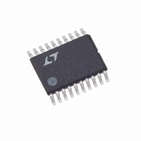
LTC3416EFE Linear Technology, LTC3416EFE Datasheet - Page 11

LTC3416EFE
Manufacturer Part Number
LTC3416EFE
Description
IC REG SYNC 4A STEPDOWN 20TSSOP
Manufacturer
Linear Technology
Type
Step-Down (Buck)r
Datasheet
1.LTC3416EFEPBF.pdf
(16 pages)
Specifications of LTC3416EFE
Internal Switch(s)
Yes
Synchronous Rectifier
Yes
Number Of Outputs
1
Voltage - Output
0.8 ~ 5 V
Current - Output
4A
Frequency - Switching
1MHz
Voltage - Input
2.25 ~ 5.5 V
Operating Temperature
-40°C ~ 85°C
Mounting Type
Surface Mount
Package / Case
20-TSSOP Exposed Pad, 20-eTSSOP, 20-HTSSOP
Lead Free Status / RoHS Status
Contains lead / RoHS non-compliant
Power - Output
-
Available stocks
Company
Part Number
Manufacturer
Quantity
Price
Part Number:
LTC3416EFE
Manufacturer:
LT/凌特
Quantity:
20 000
Part Number:
LTC3416EFE#PBF
Manufacturer:
LINEAR/凌特
Quantity:
20 000
APPLICATIO S I FOR ATIO
An alternative method of tracking is shown in Figure 5. For
the circuit of Figure 5, the following equations can be used
to determine the resistor values:
Soft-Start
The RUN/SS pin provides a means to shut down the
LTC3416 as well as a timer for soft-start. Pulling the RUN/
SS pin below 0.5V places the LTC3416 in a low quiescent
current shutdown state (I
The soft-start gradually raises the clamp on I
current range becomes available on I
on I
externally with a resistor and capacitor on the RUN/SS pin.
The soft-start duration can be calculated by using the
following formula:
R
V
V
t
TH
SS
OUT
OUT
4
=
reaches approximately 2V. The clamp on I
=
1
2
R
R C In
Figure 5. Dual Voltage System with Tracking
=
=
3
SS SS
⎛
⎜
⎝
0 8
0 8
V
.
V
.
OUT
OUT
V
V
⎛
⎜
⎝
⎛
⎜
⎝
1
2
1
1
⎛
⎜
⎝
U
+
TRACK
+
–
V
R
R
1
IN
R
MASTER
LTC3416
LTC3416
⎞
⎟
⎠
SLAVE
2
1
4
V
– .
R
⎞
⎟
⎠
+
IN
U
Q
1 8
3
SGND
SGND
R
< 1µA).
V
V
5
FB
FB
V
⎞
⎟
⎠
⎞
⎟
⎠
(
Seconds
W
V
V
OUT2
OUT1
TH
R5
R4
R3
R2
R1
3416 F05
after the voltage
)
TH
U
. The full
TH
is set
Efficiency Considerations
The efficiency of a switching regulator is equal to the
output power divided by the input power times 100%. It is
often useful to analyze individual losses to determine what
is limiting the efficiency and which change would produce
the most improvement. Efficiency can be expressed as:
where L1, L2, etc. are the individual losses as a percentage
of input power.
Although all dissipative elements in the circuit produce
losses, two main sources usually account for most of the
losses: V
The V
loss at very low load currents whereas the I
dominates the efficiency loss at medium to high load
currents. In a typical efficiency plot, the efficiency curve at
very low load currents can be misleading since the actual
power lost is of no consequence.
1. The V
2. I
Efficiency = 100% – (L1 + L2 + L3 + ...)
DC bias current as given in the electrical characteristics
and the internal main switch and synchronous switch
gate charge currents. The gate charge current results
from switching the gate capacitance of the internal power
MOSFET switches. Each time the gate is switched from
high to low to high again, a packet of charge dQ moves
from V
of V
continuous mode, I
Q
switches. Both the DC bias and gate charge losses are
proportional to V
pronounced at higher supply voltages.
internal switches, R
continuous mode the average output current flowing
through inductor L is “chopped” between the main
switch and the synchronous switch. Thus, the series
resistance looking into the SW pin is a function of both
top and bottom MOSFET R
(DC) as follows:
2
B
R losses are calculated from the resistances of the
R
IN
are the gate charges of the internal top and bottom
IN
SW
IN
quiescent current loss dominates the efficiency
that is typically larger than the DC bias current. In
IN
IN
quiescent current is due to two components: the
= (R
to ground. The resulting dQ/dt is the current out
quiescent current and I
DS(ON)TOP
IN
GATECHG
and thus their effects will be more
SW
)(DC) + (R
, and external inductor R
= f(Q
DS(ON)
2
DS(ON)BOT
T
R losses.
+ Q
and the duty cycle
LTC3416
B
) where Q
)(1 – DC)
2
11
R loss
T
L
3416fa
and
. In


