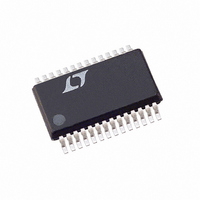
LTC3729EG Linear Technology, LTC3729EG Datasheet - Page 20

LTC3729EG
Manufacturer Part Number
LTC3729EG
Description
IC SW REG SYNC STEP-DOWN 28-SSOP
Manufacturer
Linear Technology
Series
PolyPhase®r
Type
Step-Down (Buck)r
Datasheet
1.LTC3729EGPBF.pdf
(30 pages)
Specifications of LTC3729EG
Internal Switch(s)
No
Synchronous Rectifier
Yes
Number Of Outputs
1
Voltage - Output
0.8 ~ 5 V
Current - Output
5A
Frequency - Switching
1.1MHz
Voltage - Input
4 ~ 36 V
Operating Temperature
-40°C ~ 85°C
Mounting Type
Surface Mount
Package / Case
28-SSOP
Lead Free Status / RoHS Status
Contains lead / RoHS non-compliant
Power - Output
-
Available stocks
Company
Part Number
Manufacturer
Quantity
Price
Part Number:
LTC3729EG#PBF
Manufacturer:
LINEAR/凌特
Quantity:
20 000
Company:
Part Number:
LTC3729EGN
Manufacturer:
PHILIPS
Quantity:
15
APPLICATIONS INFORMATION
LTC3729
Voltage Positioning
Voltage positioning can be used to minimize peak‑to‑peak
output voltage excursions under worst‑case transient
loading conditions. The open‑loop DC gain of the control
loop is reduced depending upon the maximum load step
specifications. Voltage positioning can easily be added to
the LTC3729 by loading the I
having a Thevenin equivalent voltage source equal to the
midpoint operating voltage range of the error amplifier, or
1.2V (see Figure 8).
The resistive load reduces the DC loop gain while main‑
taining the linear control range of the error amplifier.
The maximum output voltage deviation can theoretically
be reduced to half or alternatively the amount of output
capacitance can be reduced for a particular application.
A complete explanation is included in Design Solutions
10. (See www.linear‑tech.com)
Efficiency Considerations
The percent efficiency of a switching regulator is equal to
the output power divided by the input power times 100%.
It is often useful to analyze individual losses to determine
what is limiting the efficiency and which change would
produce the most improvement. Percent efficiency can
be expressed as:
where L1, L2, etc. are the individual losses as a percent‑
age of input power.
Although all dissipative elements in the circuit produce
losses, four main sources usually account for most of
the losses in LTC3729 circuits: 1) LTC3729 V
(including loading on the differential amplifier output),
20
Figure 8. Active Voltage Positioning Applied to the LTC3729
%Efficiency = 100% – (L1 + L2 + L3 + ...)
INTV
CC
R
R
T2
T1
R
C
C
C
TH
I
TH
pin with a resistive divider
LTC3729
3729 F08
IN
current
2) INTV
MOSFET transition losses.
1) The V
DC supply current given in the Electrical Characteristics
table, which excludes MOSFET driver and control currents;
the second is the current drawn from the differential
amplifier output. V
(<0.1%) loss.
2) INTV
control currents. The MOSFET driver current results from
switching the gate capacitance of the power MOSFETs.
Each time a MOSFET gate is switched from low to high
to low again, a packet of charge dQ moves from INTV
to ground. The resulting dQ/dt is a current out of INTV
that is typically much larger than the control circuit cur‑
rent. In continuous mode, I
Q
side MOSFETs.
Supplying INTV
from an output‑derived source will scale the V
required for the driver and control circuits by the ratio (Duty
Factor)/(Efficiency). For example, in a 20V to 5V application,
10mA of INTV
V
or more (if the driver was powered directly from V
only a few percent.
3) I
fuse (if used), MOSFET, inductor, current sense resistor,
and input and output capacitor ESR. In continuous
mode the average output current flows through L and
R
and the synchronous MOSFET. If the two MOSFETs have
approximately the same R
one MOSFET can simply be summed with the resistances
of L, R
if each R
then the total resistance is 25mΩ. This results in losses
ranging from 2% to 8% as the output current increases
from 3A to 15A per output stage for a 5V output, or a 3%
to 12% loss per output stage for a 3.3V output. Efficiency
varies as the inverse square of V
components and output power level. The combined effects
IN
T
SENSE
and Q
2
current. This reduces the mid‑current loss from 10%
R losses are predicted from the DC resistances of the
SENSE
, but is “chopped” between the topside MOSFET
CC
CC
IN
B
DS(ON)
regulator current, 3) I
are the gate charges of the topside and bottom
current is the sum of the MOSFET driver and
current has two components: the first is the
and ESR to obtain I
CC
CC
=10mΩ, R
current results in approximately 3mA of
power through the EXTV
IN
current typically results in a small
DS(ON)
L
=10mΩ, and R
GATECHG
OUT
2
2
R losses and 4) Topside
, then the resistance of
R losses. For example,
for the same external
= (Q
T
CC
+ Q
SENSE
switch input
IN
B
), where
current
=5mΩ,
IN
3729fb
) to
CC
CC


