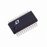
LTC1436AIGN Linear Technology, LTC1436AIGN Datasheet - Page 8

LTC1436AIGN
Manufacturer Part Number
LTC1436AIGN
Description
IC SW REG SYNC STEP-DOWN 24-SSOP
Manufacturer
Linear Technology
Type
Step-Down (Buck)r
Datasheet
1.LTC1436AIGN-PLLPBF.pdf
(28 pages)
Specifications of LTC1436AIGN
Internal Switch(s)
No
Synchronous Rectifier
Yes
Number Of Outputs
1
Voltage - Output
1.19 ~ 9 V
Current - Output
50mA
Frequency - Switching
125kHz ~ 240kHz
Voltage - Input
3.5 ~ 30 V
Operating Temperature
-40°C ~ 85°C
Mounting Type
Surface Mount
Package / Case
24-SSOP
Lead Free Status / RoHS Status
Contains lead / RoHS non-compliant
Power - Output
-
Available stocks
Company
Part Number
Manufacturer
Quantity
Price
Part Number:
LTC1436AIGN#PBF
Manufacturer:
LINEAR/凌特
Quantity:
20 000
Company:
Part Number:
LTC1436AIGN-PLL
Manufacturer:
Linear Technology
Quantity:
135
Part Number:
LTC1436AIGN-PLL
Manufacturer:
LT/凌特
Quantity:
20 000
Part Number:
LTC1436AIGN-PLL#PBF
Manufacturer:
LINEAR/凌特
Quantity:
20 000
PIN
LTC1436A
LTC1436-PLL-A/LTC1437A
Forcing this pin below 1.3V causes the device to be shut
down. In shutdown all functions are disabled.
TGL: High Current Gate Drive for Main Top N-Channel
MOSFET. This is the output of a floating driver with a
voltage swing equal to INTV
switch node voltage SW.
TGS: High Current Gate Drive for a Small Top N-Channel
MOSFET. This is the output of a floating driver with a
voltage swing equal to INTV
switch node voltage SW. Leaving TGS open invokes Burst
Mode operation at low load currents.
BG: High Current Gate Drive for Bottom N-Channel
MOSFET. Voltage swing at this pin is from ground to
INTV
SFB: Secondary Winding Feedback Input. Normally
connected to a feedback resistive divider from the
secondary winding. This pin should be tied to: ground to
force continuous operation; INTV
don’t use a secondary winding; and a resistive divider from
the output in applications using a secondary winding.
POR: Open Drain Output of an N-Channel Pull-Down. This
pin sinks current when the output voltage is 7.5% out of
regulation and releases 65536 oscillator cycles after the
output voltage rises to – 5% of its regulated value. The
POR output is asserted when Run/SS is low independent
of V
LBO: Open Drain Output of an N-Channel Pull-Down. This
pin will sink current when the LBI pin goes below 1.19V.
8
U
OUT
CC
FUNCTIONS
.
(DRV
U
CC
).
U
CC
CC
CC
superimposed on the
superimposed on the
in applications that
LBI: The (+) Input of the Low Battery Voltage Comparator.
The (–) input is connected to a 1.19V reference.
PLLIN: External Synchronizing Input to Phase Detector.
This pin is internally terminated to SGND with 50kΩ. Tie
this pin to SGND in applications which do not use the
phase-locked loop.
PLL LPF: Output of Phase Detector and Control Input of
Oscillator. Normally a series RC lowpass filter network is
connected from this pin to ground. Tie this pin to SGND in
applications which do not use the phase-locked loop. Can
be driven by 0V to 2.4V logic signal for a frequency shifting
option.
AUXFB: Feedback Input to the Auxiliary Regulator/
Comparator. When used as a linear regulator, this input
can either be connected to an external resistive divider or
directly to the collector of the external PNP pass device for
12V operation. When used as a comparator, this is the
noninverting input of a comparator whose inverting input
is tied to the internal 1.19V reference. See Auxiliary
Regulator/Comparator in Applications Information section.
AUXON: Pulling this pin high turns on the auxiliary regulator/
comparator. The threshold is 1.19V.
AUXDR: Open Drain Output of the Auxiliary Regulator/
Comparator. The base of an external PNP device is
connected to this pin for use as a linear regulator. An
external pull-up resistor is required for use as a comparator.
A voltage > 9.5V on AUXDR causes the internal 12V
resistive divider to be connected to AUXFB.
14367afb


