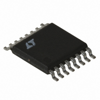
LT3430IFE#TR Linear Technology, LT3430IFE#TR Datasheet - Page 6

LT3430IFE#TR
Manufacturer Part Number
LT3430IFE#TR
Description
IC REG SW STDN 3A 200KHZ 16TSSOP
Manufacturer
Linear Technology
Type
Step-Down (Buck)r
Datasheet
1.LT3430EFE-1PBF.pdf
(28 pages)
Specifications of LT3430IFE#TR
Internal Switch(s)
Yes
Synchronous Rectifier
No
Number Of Outputs
1
Voltage - Output
1.2 ~ 54 V
Current - Output
3A
Frequency - Switching
200kHz
Voltage - Input
5.5 ~ 60 V
Operating Temperature
-40°C ~ 125°C
Mounting Type
Surface Mount
Package / Case
16-TSSOP Exposed Pad, 16-eTSSOP, 16-HTSSOP
Lead Free Status / RoHS Status
Contains lead / RoHS non-compliant
Power - Output
-
Available stocks
Company
Part Number
Manufacturer
Quantity
Price
LT3430/LT3430-1
PIN FUNCTIONS
6
GND (Pins 1, 8, 9, 16, 17): The GND pin connections act
as the reference for the regulated output, so load regulation
will suffer if the “ground” end of the load is not at the same
voltage as the GND pins of the IC. This condition will occur
when load current or other currents fl ow through metal
paths between the GND pins and the load ground. Keep the
paths between the GND pins and the load ground short and
use a ground plane when possible. The FE package has an
exposed pad that is fused to the GND pins. The pad (Pin
17) should be soldered to the copper ground plane under
the device to reduce thermal resistance. (See Applications
Information—Layout Considerations.)
SW (Pins 2, 5): The switch pin is the emitter of the on-chip
power NPN switch. This pin is driven up to the input pin
voltage during switch on time. Inductor current drives the
switch pin voltage negative during switch off time. Negative
voltage is clamped with the external catch diode. Maximum
negative switch voltage allowed is –0.8V.
V
NPN switch. V
a voltage on the BIAS pin is not present. High dI/dt edges
occur on this pin during switch turn on and off. Keep the
path short from the V
capacitor, through the catch diode back to SW. All trace
inductance in this path creates voltage spikes at switch
off, adding to the V
BOOST (Pin 6): The BOOST pin is used to provide a drive
voltage, higher than the input voltage, to the internal bipolar
NPN power switch. Without this added voltage, the typical
switch voltage loss would be about 1.5V. The additional
BOOST voltage allows the switch to saturate and voltage
loss approximates that of a 0.1Ω FET structure.
NC (Pins 7, 13): No Connection.
BIAS (Pin 10): The BIAS pin is used to improve effi ciency
when operating at higher input voltages and light load cur-
rent. Connecting this pin to the regulated output voltage
forces most of the internal circuitry to draw its operating
current from the output voltage rather than the input supply.
IN
(Pins 3, 4): This is the collector of the on-chip power
IN
powers the internal control circuitry when
CE
voltage across the internal NPN.
IN
pin through the input bypass
This architecture increases effi ciency especially when the
input voltage is much higher than the output. Minimum
output voltage setting for this mode of operation is 3V.
V
and the input of the peak switch current comparator. It is
normally used for frequency compensation, but can also
serve as a current clamp or control loop override. V
at about 0.9V for light loads and 2.1V at maximum load.
It can be driven to ground to shut off the regulator, but if
driven high, current must be limited to 4mA.
FB (Pin 12): The feedback pin is used to set the output
voltage using an external voltage divider that generates
1.22V at the pin for the desired output voltage. Three
additional functions are performed by the FB pin. When
the pin voltage drops below 0.6V, switch current limit is
reduced and the external SYNC function is disabled. Below
0.8V, switching frequency is also reduced. See Feedback
Pin Functions in Applications Information for details.
SYNC (Pin 14): The SYNC pin is used to synchronize the
internal oscillator to an external signal. It is directly logic
compatible and can be driven with any signal between 10%
and 90% duty cycle. The synchronizing range is 125kHz
to 250kHz for the LT3430-1 and 228kHz to 700kHz for the
LT3430. See Synchronizing in Applications Information
for details.
⎯ S ⎯ H ⎯ D ⎯ N (Pin 15): The ⎯ S ⎯ H ⎯ D ⎯ N pin is used to turn off the
regulator and to reduce input drain current to a few mi-
croamperes. This pin has two thresholds: one at 2.38V to
disable switching and a second at 0.4V to force complete
micropower shutdown. The 2.38V threshold functions
as an accurate undervoltage lockout (UVLO); sometimes
used to prevent the regulator from delivering power until
the input voltage has reached a predetermined level.
If the ⎯ S ⎯ H ⎯ D ⎯ N pin functions are not required, the pin can
either be left open (to allow an internal bias current to lift
the pin to a default high state) or be forced high to a level
not to exceed 6V.
C
(Pin 11): The V
C
pin is the output of the error amplifi er
C
34301fa
sits


