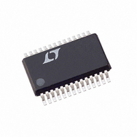
LTC1538CG-AUX Linear Technology, LTC1538CG-AUX Datasheet - Page 8

LTC1538CG-AUX
Manufacturer Part Number
LTC1538CG-AUX
Description
IC SW REG STP-DN SYNC DUAL28SSOP
Manufacturer
Linear Technology
Type
Step-Down (Buck)r
Specifications of LTC1538CG-AUX
Internal Switch(s)
No
Synchronous Rectifier
Yes
Number Of Outputs
2
Voltage - Output
1.19 ~ 9 V
Current - Output
50mA
Frequency - Switching
125kHz ~ 240kHz
Voltage - Input
3.5 ~ 36 V
Operating Temperature
0°C ~ 70°C
Mounting Type
Surface Mount
Package / Case
28-SSOP
Lead Free Status / RoHS Status
Contains lead / RoHS non-compliant
Power - Output
-
Available stocks
Company
Part Number
Manufacturer
Quantity
Price
Part Number:
LTC1538CG-AUX
Manufacturer:
LT/凌特
Quantity:
20 000
Part Number:
LTC1538CG-AUX#PBF
Manufacturer:
LINEAR/凌特
Quantity:
20 000
Company:
Part Number:
LTC1538CG-AUX-TR
Manufacturer:
FUJI
Quantity:
500
Part Number:
LTC1538CG-AUX-TR
Manufacturer:
LT/凌特
Quantity:
20 000
SENSE
Comparator. Built-in offsets between SENSE
SENSE
trip threshold (same for second controller).
V
the second controller either from the output directly or from
an external resistive divider across the output . The V
pin determines which point. V
V
for Output Voltage Sensing. The voltage sensing for the
first controller is internally connected to SENSE
the V
controller. For V
set for an output voltage of 3.3V. With V
V
voltage of 5V. Leaving V
voltage of the second controller to be set by an external
resistive divider connected to V
C
the operating frequency.
I
sociated current comparator threshold increases with this
control voltage.
RUN/SS1, RUN/SS2: Combination of Soft Start and RUN
Control Inputs. A capacitor to ground at each of these pins
sets the ramp time to full current output. The time is
approximately 0.5s/ F. Forcing either of these pins below
1.3V causes the IC to shut down the circuitry required for
that particular controller. Forcing both of these pins below
1.3V causes the device to shut down both controllers,
leaving the 5V standby regulator, internal reference and a
comparator active. Refer to the LTC1438/LTC1439 for appli-
cations which do not require a 5V standby regulator.
TGL1, TGL2: High Current Gate Drives for Main Top
N-Channel MOSFET. These are the outputs of floating
drivers with a voltage swing equal to INTV
posed on the switch node voltage SW1 and SW2.
TGS1, TGS2: Gate Drives for Small Top N-Channel
MOSFET. These are the outputs of floating drivers with a
voltage swing equal to INTV
switch node voltage SW. Leaving TGS1 or TGS2 open
invokes Burst Mode operation for that controller.
LTC1538-AUX/LTC1539
PIN
8
TH1
OSENSE2
PROG1
PROG2
OSC
U
, I
OSENSE2
: External capacitor C
TH2
+
FUNCTIONS
+
, V
> V
1 pins in conjunction with R
: Receives the remotely sensed feedback voltage for
1, SENSE
: Error Amplifier Compensation Point. Each as-
PROG2
U
INTVCC
pin allows for remote sensing for the second
PROG1
: Programs Internal Voltage Attenuators
/1.5 the divider is set for an output
+
U
2: The (+) Input to Each Current
, V
PROG2
PROG2
OSC
OSENSE2
open (DC) allows the output
from this pin to ground sets
CC
< V
OSENSE2
superimposed on the
INTVCC
SENSE1
must connect to.
.
/3, the divider is
set the current
CC
superim-
–
–
1 while
PROG1
1 and
PROG2
,
BG1, BG2: High Current Gate Drive Outputs for Bottom N-
Channel MOSFETs. Voltage swing at these pins is from
ground to INTV
SFB1: Secondary Winding Feedback Input. This input acts
only on the first controller and is normally connected to a
feedback resistive divider from the secondary winding.
Pulling this pin below 1.19V will force continuous syn-
chronous operation for the first controller. This pin should
be tied to: ground to force continuous operation; INTV
in applications that don’t use a secondary winding; and a
resistive divider from the output in applications using a
secondary winding.
POR1: This output is a drain of an N-channel pull-down.
This pin sinks current when the output voltage of the first
controller drops 7.5% below its regulated voltage and re-
leases 65536 oscillator cycles after the output voltage of the
first controller rises to within –5% value of its regulated value.
The POR1 output is asserted when RUN/SS1 and RUN/SS2
are both low, independent of the V
LBO: This output is a drain of an N-channel pull-down. This
pin will sink current when the LBI pin goes below 1.19V
irrespective of the RUN/SS pin voltage.
LBI: The (+) input of a comparator which can be used as
a low-battery voltage detector irrespective of the RUN/SS
pin voltage. The (–) input is connected to the 1.19V
internal reference.
PLLIN: External Synchronizing Input to Phase Detector.
This pin is internally terminated to SGND with 50k . Tie
this pin to SGND in applications which do not use the
phase-locked loop.
PLL LPF: Output of Phase Detector and Control Input of
Oscillator. Normally a series RC lowpass filter network is
connected from this pin to ground. Tie this pin to SGND in
applications which do not use the phase-locked loop. Can
be driven by a 0V to 2.4V logic signal for a frequency
shifting option.
AUXFB: Feedback Input to the Auxiliary Regulator/Com-
parator. When used as a linear regulator, this input can
either be connected to an external resistive divider or
directly to the collector of the external PNP pass device for
12V operation. When used as a comparator, this is the
CC
.
OUT1
.
CC


