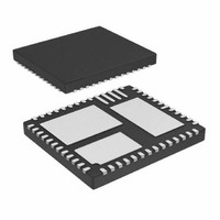
LTC3609IWKG#TRPBF Linear Technology, LTC3609IWKG#TRPBF Datasheet - Page 18

LTC3609IWKG#TRPBF
Manufacturer Part Number
LTC3609IWKG#TRPBF
Description
IC DC/DC CONV STP-DWN 6A 52-QFN
Manufacturer
Linear Technology
Type
Step-Down (Buck)r
Datasheet
1.LTC3609EWKGPBF.pdf
(26 pages)
Specifications of LTC3609IWKG#TRPBF
Internal Switch(s)
Yes
Synchronous Rectifier
Yes
Number Of Outputs
2
Voltage - Output
0.6 ~ 36 V
Current - Output
6A
Voltage - Input
4 ~ 32 V
Operating Temperature
-40°C ~ 125°C
Mounting Type
Surface Mount
Package / Case
52-QFN
Lead Free Status / RoHS Status
Lead free / RoHS Compliant
Power - Output
-
Frequency - Switching
-
Available stocks
Company
Part Number
Manufacturer
Quantity
Price
LTC3609
applicaTions inForMaTion
Design Example
As a design example, take a supply with the following
specifications: V
2.5V ± 5%, I
timing resistor with V
and choose the inductor for about 40% ripple current at
the maximum V
Selecting a standard value of 1.5µH results in a maximum
ripple current of:
L =
R
ΔI
(
ON
550kHz
L
=
5V TO 32V
=
(
2.5V AT
(
550kHz
2 4
V
GND
2.5V
OUT
V
OUT(MAX)
.
6A
IN
)
( )
V
0.4
C
100µF
2.5V
)(
IN
OUT1
IN
C
C
L
KEEP POWER GROUND AND SIGNAL
GROUND SEPARATE. CONNECT AT
ONE POINT.
x2
:
550
)
IN
OUT
I
: CDEP851R2MC-50
C
4.7µF
50V
x2
(
: MURATA GRM32ER71H475K
( )
2 5
+
IN
= 5V to 32V (12V nominal), V
1.5µH
6A
: MURATA GRM435R60J107M
.
= 6A, f = 550kHz. First, calculate the
ON
kHz
V
1.2µH
L1
= V
1−
)(
)
V
IN
10
OUT
1–
2.5V
32V
GND
pF
41
42
43
44
45
46
47
48
49
50
51
52
Figure 6. Design Example: 5V to 32V Input to 2.5V/6A at 550kHz
:
2.5V
12V
)
SW
SW
SW
SW
SW
SW
SW
PV
PV
PV
PV
PV
=1.8µH
=
IN
IN
IN
IN
IN
1
40 39 38 37 36 35 34 33
187
= 2.4A
2
k
3
INTV
4
CC
5
4.7µF
CMDSH-3
C
6.3V
6
VCC
D
B
7
OUT
LTC3609
8
SW
SW
=
SW
9 10 11
INTV
32
C
0.22µF
CC
31
B1
0.1µF
Next, set up V
to GND will set the typical current limit to 9A, and tying
V
C
85°C. The ceramic output capacitors are chosen for an
ESR of 0.002Ω to minimize output voltage changes due
to inductor ripple current and load steps. The ripple volt-
age is:
and a 0A to 6A load step will only cause an output
change of:
An optional 22µF ceramic output capacitor is included
to minimize the effect of ESL in the output ripple. The
complete circuit is shown in Figure 6.
30 29 28 27
C
RNG
IN
SS
∆V
2
∆V
12 13 14
is chosen for an RMS current rating of about 5A at
OUT(STEP)
OUT(RIPPLE)
to 1.2V will result in a typical current around 14A.
C
0.1µF
50V
F
PGOOD
C
0.1µF
SGND
SGND
SGND
VON
V
FCB
RNG
V
I
I
NC
NC
NC
ON
TH
R
FB
1
RNG
F1
= ∆I
26
25
24
23
22
21
20
19
18
17
16
15
= ∆I
= (2.4A) (0.002Ω) = 4.8mV
voltage and check the I
V
IN
LOAD
SGND
V
L(MAX)
OUT
(ESR) = (6A) (0.002Ω) = 12mV
R1
9.53k
1%
PGOOD
C4
0.01µF
(ESR)
EXTV
R
100k
PG1
30.1k
187k
R
CC
1%
1%
R2
ON
15.8k
INTV
R5
CC
1000pF
V
V
100pF
OUT
IN
C
C
LIMIT
C1
C2
. Tying V
INTV
3609 F06
CC
JP1
3609fb
RNG


