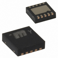
MIC2202-1.5YML Micrel Inc, MIC2202-1.5YML Datasheet - Page 7

MIC2202-1.5YML
Manufacturer Part Number
MIC2202-1.5YML
Description
IC REG PWM SYNC 2MHZ 1.5V 10-MLF
Manufacturer
Micrel Inc
Type
Step-Down (Buck)r
Datasheet
1.MIC2202YMM.pdf
(19 pages)
Specifications of MIC2202-1.5YML
Internal Switch(s)
Yes
Synchronous Rectifier
No
Number Of Outputs
1
Voltage - Output
1.5V
Current - Output
600mA
Frequency - Switching
2MHz
Voltage - Input
2.3 ~ 5.5 V
Operating Temperature
-40°C ~ 125°C
Mounting Type
Surface Mount
Package / Case
10-MLF®, QFN
Lead Free Status / RoHS Status
Lead free / RoHS Compliant
Power - Output
-
Application Information
Input Capacitor
A minimum 1µF ceramic is recommended on the VIN pin
for bypassing. X5R or X7R dielectrics are recommended
for the input capacitor. Y5V dielectrics, aside from losing
most of their capacitance over temperature, they also
become resistive at high frequencies. This reduces their
ability to filter out high frequency noise.
Output Capacitor
The MIC2202 was designed specifically for the use of a
1µF ceramic output capacitor. This value can be
increased to improve transient performance. Since the
MIC2202 is voltage mode, the control loop relies on the
inductor and output capacitor for compensation. For this
reason, do not use excessively large output capacitors.
The output capacitor requires either an X7R or X5R
dielectric. Y5V and Z5U dielectric capacitors, aside from
the undesirable effect of their wide variation in
capacitance over temperature, become resistive at high
frequencies. Using Y5V or Z5U capacitors will cause
instability in the MIC2202.
Total output capacitance should not exceed 15µF. Large
values of capacitance can cause current limit to engage
during start-up. If larger than 15µF is required, a feed-
forward capacitor from the output to the feedback node
should be used to slow the start up time.
Inductor Selection
Inductor selection will be determined by the following
(not necessarily in the order of importance):
The MIC2202 is designed for use with a 1µH to 4.7µH
inductor.
Maximum current ratings of the inductor are generally
given in two methods: permissible DC current and
saturation current. Permissible DC current can be rated
either for a 40°C temperature rise or a 10% loss in
inductance. Ensure the inductor selected can handle the
maximum operating current. When saturation current is
specified, make sure that there is enough margin that
the peak current will not saturate the inductor.
The size requirements refer to the area and height
requirements that are necessary to fit a particular
design. Please refer to the inductor dimensions on their
datasheet.
DC resistance is also important. While DCR is inversely
proportional to size, DCR can represent a significant
efficiency loss. Refer to the “Efficiency Considerations”
Micrel, Inc.
March 2007
•
•
•
•
Inductance
Rated current value
Size requirements
DC resistance (DCR)
7
below for a more detailed description.
Bias Capacitor
A small 10nF ceramic capacitor is required to bypass the
bias pin. The use of low ESR ceramics provides
improved filtering for the bias supply.
Efficiency Considerations
Efficiency is defined as the amount of useful output
power, divided by the amount of power consumed.
Maintaining high efficiency serves two purposes. It
reduces power dissipation in the power supply, reducing
the need for heat sinks and thermal design considera-
tions and it reduces consumption of current for battery
powered applications. Reduced current draw from a
battery increases the devices operating time, critical in
hand held devices.
There are two loss terms in switching converters: DC
losses and switching losses. DC losses are simply the
power dissipation of I
side switch during the on cycle. Power loss is equal to
the high side MOSFET RDS
Current
MOSFET conducts, also dissipating power. Device
operating current also reduces efficiency. The product of
the quiescent (operating) current and the supply voltage
is another DC loss. The current required to drive the
gates on and off at a constant 2MHz frequency and the
switching transitions make up the switching losses.
Figure 2 shows an efficiency curve. The non-shaded
portion, from 0mA to 200mA, efficiency losses are
dominated by quiescent current losses, gate drive and
transition losses. In this case, lower supply voltages
yield greater efficiency in that they require less current to
drive the MOSFETs and have reduced input power
consumption.
2
Efficiency % =
. During the off cycle, the low side N-Channel
100
Figure 2. Efficiency Curve
95
90
85
80
75
70
65
60
55
50
0
vs. Output Current
4.2V
0.1 0.2 0.3 0.4 0.5 0.6
2
OUTPUT CURRENT (A)
R. Power is dissipated in the high
⎛
⎜ ⎜
⎝
V
IN
Efficiency
OUT
V
IN
(ON)
×
×
I
I
5V
IN
OUT
multiplied by the Switch
3.3V
IN
⎞
⎟ ⎟
⎠
OUT
×
100
M9999-031907
MIC2202


