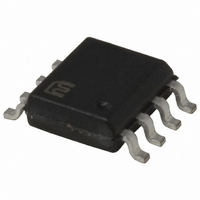
MIC4684-3.3BM TR Micrel Inc, MIC4684-3.3BM TR Datasheet - Page 11

MIC4684-3.3BM TR
Manufacturer Part Number
MIC4684-3.3BM TR
Description
IC REG BUCK HI EFF 2A 3.3V 8SOIC
Manufacturer
Micrel Inc
Series
SuperSwitcher™r
Type
Step-Down (Buck)r
Datasheet
1.MIC4684-3.3BM_TR.pdf
(16 pages)
Specifications of MIC4684-3.3BM TR
Internal Switch(s)
Yes
Synchronous Rectifier
No
Number Of Outputs
1
Voltage - Output
3.3V
Current - Output
2A
Frequency - Switching
200kHz
Voltage - Input
4 ~ 30 V
Operating Temperature
-40°C ~ 125°C
Mounting Type
Surface Mount
Package / Case
8-SOIC (3.9mm Width)
Lead Free Status / RoHS Status
Contains lead / RoHS non-compliant
Power - Output
-
Other names
MIC4684-3.3BMTR
MIC4684-3.3BMTR
MIC4684-3.3BMTR
A worst-case rule of thumb is to assume that 80% of the total
output power dissipation is in the MIC4684 (P
is in the diode-inductor-capacitor circuit.
Calculate the worst-case junction temperature:
where:
The θ
25°C/W.
entry point of pins 2, 6 or 7
for the specific design.
Calculating the maximum junction temperature given a
maximum ambient temperature of 60°C:
January 2010
MIC4684
P
P
P
T
T
P
θ
JC
T
T
T
T
T
JC
A
A(max)
J
J
C
J
J
D(IC)
D(IC)
D(IC)
D(IC)
for the MIC4684’s power-SOP-8 is approximately
= P
= MIC4684 junction temperature
= ambient temperature
= 0.76 × 25°C/W + (41°C – 25°C) + 60°C
= 95°C
= “pin” temperature measurement taken at the
= junction-to-case thermal resistance.
D(IC)
= 0.8 P
= 0.8 × 0.95W
= 0.76W
= MIC4684 power dissipation
= maximum ambient operating temperature
θ
JC
D
+ (T
C
– T
A
) + T
(34V transient)
+4V to +30V
Power
SOP-8
A(max)
V
IN
C
IN
Figure 5. Critical Traces for Layout
D(IC)
3
8
IN
EN
) and 20%
MIC4684BM
2
GND
6
7
SW
BS
FB
11
4
1
5
This value is within the allowable maximum operating junction
temperature of 125°C as listed in “Operating Ratings.” Typical
thermal shutdown is 160°C and is listed in Electrical Charac-
teristics. Also see SOA curves on pages 7 through 8.
Layout Considerations
Layout is very important when designing any switching regu-
lator. Rapidly changing currents through the printed circuit
board traces and stray inductance can generate voltage
transients which can cause problems.
To minimize stray inductance and ground loops, keep trace
lengths as short as possible. For example, keep D1 close
to pin 1 and pins 2, 6, and 7, keep L1 away from sensitive
node FB, and keep C
See Applications Information: Thermal Considerations for
ground plane layout.
The feedback pin should be kept as far way from the switch-
ing elements (usually L1 and D1) as possible.
A circuit with sample layouts are provided. See Figure 7.
Gerber files are available upon request.
Feed Forward Diode
The FF diode (feed forward) provides an external bias source
directly to the main pass element, this reduces V
allowing the MIC4684 to be used in very low head-room ap-
plications I.E. 5V
D1
68µH
L1
C
OUT
IN
to 3.3V
R1
R2
V
GND
IN
OUT
close to pin 3 and pins 2, 6, and 7.
OUT.
M9999-012610
Micrel, Inc.
SAT
thus


