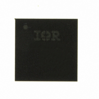
IP2005ATRPBF International Rectifier, IP2005ATRPBF Datasheet

IP2005ATRPBF
Specifications of IP2005ATRPBF
Available stocks
Related parts for IP2005ATRPBF
IP2005ATRPBF Summary of contents
Page 1
... General DC/DC Converters Package Interface Standard Quantity Description Connection iP2005APbF LGA iP2005ATRPbF LGA 2000 Typical Application www.irf.com High Frequency Synchronous Buck Optimized LGA Power Stage Integrated Power Semiconductors, Driver IC, & Passives = 95ºC Description The iP2005A is a fully optimized solution for high current synchronous buck multiphase applications ...
Page 2
ABSOLUTE MAXIMUM RATINGS (Voltages referenced to P GND …………………………..…..-0.5V to 16.5V IN GND ………………….…….…….-0.5V to 7.5V DD GND ……..….……..…………...-0.5V to 7.5V CC GND PWM to P …………………….………-0.5V to VDD + 0.5V ...
Page 3
Electrical Specifications These specifications apply for T PARAMETER P LOSS Power Block Losses V DD Supply Current (Stand By Q-VDD Supply Current (Operating) CV (LDO Output) CC Output Voltage Output Current Output Capacitor Power-On Reset (POR) V Rising ...
Page 4
Electrical Specifications (continued) These specifications apply for T PARAMETER PWM INPUT Logic Level Low Threshold ( Logic Level High Threshold ( Threshold Hysteresis Weak Pull-down impedance Rising Propagation Delay (T ) PDH Falling Propagation Delay (T ...
Page 5
Power Loss Curve SOA Curve www.irf.com Figure 1 Power Loss Curve Figure 2 Safe Operating Area Curve 2/8/2008 PD-60325 iP2005APbF 5 ...
Page 6
Typical Performance Curves 1. 5. 1.3V OUT I = 40A OUT F = 1MHz 1. 300nH OUT T = 125ºC BLK 1.04 1.02 1.00 0.98 0.96 0.94 0.92 0. ...
Page 7
Figure 8 Power Loss Test Circuit Figure 9 Timing Diagram 2/8/2008 PD-60325 iP2005APbF 7 ...
Page 8
... It incorporates the ability to solve thermal problems where heat is drawn out through the printed circuit board and the top of the case. Please refer to International Rectifier Application Note AN1047 for further details on using this SOA curve in your thermal environment ...
Page 9
Calculating Power Loss and SOA for Different Operating Conditions To calculate Power Loss for a given set of operation conditions, the following procedure should be followed: Power Loss Procedure 1.Determine the maximum current for each iP2005A and obtain the maximum ...
Page 10
Calculating SOA Temperature: (Figure 3) (Figure 4) (Figure 5) (Figure 6) axis intercept adjustment ≈ -1.2 ºC + 0.0 ºC + 0.6 ºC – 3.5 ºC ≈ -4.1 º Assuming T = 100ºC & T PCB The following ...
Page 11
Optimized EMI Feature 5V/div 20nS/div Vsw of iP2003A The iP2005A is designed for low Electromagnetic Interference (EMI) which minimizes power loss and space, and simplifies system design by eliminating the need for external snubber circuits. These benefits are achieved by ...
Page 12
Internal Block Diagram Pin Description Pin Number Pin Name Vsw 3 P GND PWM 6 ENABLE www.irf.com Figure 11 Internal Block Diagram Description Input voltage pin. Connect input ...
Page 13
Recommended PCB Layout Figure 12 Top copper and Solder-mask layer of PCB layout www.irf.com 2/8/2008 PD-60325 iP2005APbF 13 ...
Page 14
... The following guidelines are recommended to reduce the parasitic values and optimize overall performance. • All pads on the iP2005A footprint design need to be Solder-mask defined (see Figure 12). Also refer to International Rectifier application notes AN1028 and AN1029 for further footprint design guidance. • Place as many vias around the Power pads (V optimal thermal performance. • ...
Page 15
Mechanical Outline Drawing C 0. CORNER ID TOP VIEW ENABLE 6 PWM BOTTOM VIEW ELECTRICAL I/O www.irf.com 4 0. SIDE VIEW 5 Notes ...
Page 16
Tape and Reel Information YYMM XXXX 2005AP www.irf.com YYMM XXXX 2005AP XX XX 12.00 (.473) FEED DIRECTION Figure 15 Tape and Reel Information 2/8/2008 PD-60325 iP2005APbF 16.00 (.630) 16 ...
Page 17
Recommended Solder Paste Stencil Design CORNER ID Notes: 1.This view is stencil squeegee view 2.Dimensions are shown in millimeters 3.This opening is based on using 150 micron thick stencil. If using a different thickness stencil, this opening needs to be ...
Page 18
IR WORLD HEADQUARTERS: www.irf.com 101 N. Sepulveda Blvd., El Segundo, California 90245, USA Tel: (310) 252-7105 This product has been designed for the Industrial market. Visit us at www.irf.com for sales contact information Data and specifications subject to change without ...


