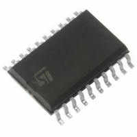
L4973D5.1 STMicroelectronics, L4973D5.1 Datasheet - Page 4

L4973D5.1
Manufacturer Part Number
L4973D5.1
Description
IC REG SW 3.5A STEPDOWN 20-SOIC
Manufacturer
STMicroelectronics
Type
Step-Down (Buck)r
Specifications of L4973D5.1
Internal Switch(s)
Yes
Synchronous Rectifier
No
Number Of Outputs
1
Voltage - Output
5.1V, 5.1 ~ 50 V
Current - Output
3.5A
Frequency - Switching
100kHz ~ 300kHz
Voltage - Input
8 ~ 55 V
Operating Temperature
-40°C ~ 150°C
Mounting Type
Surface Mount
Package / Case
20-SOIC (7.5mm Width)
Power - Output
4W
Output Voltage
5.1 V
Output Current
3.5 A
Input Voltage
8 V to 55 V
Switching Frequency
90 KHz to 110 KHz
Operating Temperature Range
- 40 C to + 150 C
Mounting Style
SMD/SMT
Duty Cycle (max)
97 %
Current, Input Bias
2 μA
Current, Output
300 μA
Current, Supply
2.7 mA
Frequency, Oscillator
100 kHz
Package Type
SO-20
Power Dissipation
4 W
Regulation, Line
5 mV
Regulation, Load
2 mV
Regulator Type
Switching
Temperature, Operating, Range
-40 to +150 °C
Transconductance
2.5
Voltage, Gain
60 dB
Voltage, Input
55 V
Voltage, Output
5.1 V
Voltage, Output, High
3 V
Voltage, Output, Low
0.8 V
Voltage, Supply
24 V
For Use With
497-4743 - BOARD EVAL FOR L4973X SW REG
Lead Free Status / RoHS Status
Lead free / RoHS Compliant
Other names
497-1412-5
Available stocks
Company
Part Number
Manufacturer
Quantity
Price
Company:
Part Number:
L4973D5.1
Manufacturer:
ST
Quantity:
3 393
Part Number:
L4973D5.1
Manufacturer:
ST
Quantity:
20 000
Company:
Part Number:
L4973D5.1-013TR
Manufacturer:
TI
Quantity:
6 249
Part Number:
L4973D5.1-013TR
Manufacturer:
ST
Quantity:
20 000
Pin settings
2.2
Note:
4/28
1
Pin description
Table 1.
The maximum power dissipation of the package must be observed.
13,14,15
DIP-18
4,5,6
7,8
2,3
11
10
18
12
16
9
1
N° Pin
Pin description
14,15,16,17
4,5,6,7
SO-20
8,9
2,3
12
11
10
20
13
18
1
COMP
BOOT
SYNC
Name
GND
OSC
OUT
V5.1
VFB
V
INH
CC
E/A output to be used for frequency compensation
A logic signal (active high) disables the device (sleep
mode operation). If not used it must be connected to
GND; if floating the device is disabled.
A capacitor connected between this pin and the output
allows to drive the internal D-MOS.
Input/Output synchronization.
Unregulated DC input voltage
Stepdown regulator output.
Stepdown feedback input. Connecting the output
directly to this pin results in an output voltage of 3.3 V
for the L4973V3.3 and 5.1 V for L4973V5.1. An external
resistive divider is required for higher output voltages.
For output voltage resistive divider is required for higher
output voltages. For output voltage less than 3.3 V, see
Note: 1
Reference voltage externally available.
Signal ground
An external resistor connected between the unregulated
input voltage and Pin 1 and a capacitor connected from
Pin 1 to ground fixes the switching frequency. (Line feed
forward is automatically obtained)
and
Figure 33.
Description
L4973


