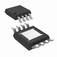
LM5085MY/NOPB National Semiconductor, LM5085MY/NOPB Datasheet - Page 19

LM5085MY/NOPB
Manufacturer Part Number
LM5085MY/NOPB
Description
IC BUCK ADJ 8MSOPEP
Manufacturer
National Semiconductor
Series
PowerWise®r
Type
Step-Down (Buck)r
Datasheet
1.LM5085MYENOPB.pdf
(22 pages)
Specifications of LM5085MY/NOPB
Design Resources
LM(2)5085 Quick Start Calculator
Internal Switch(s)
No
Synchronous Rectifier
No
Number Of Outputs
1
Voltage - Output
1.25 ~ 75 V
Frequency - Switching
Up to 1MHz
Voltage - Input
4.5 ~ 75 V
Operating Temperature
-40°C ~ 125°C
Mounting Type
Surface Mount
Package / Case
8-MSOP Exposed Pad, 8-HMSOP, 8-eMSOP
Lead Free Status / RoHS Status
Lead free / RoHS Compliant
Current - Output
-
Power - Output
-
Other names
LM5085MY
Available stocks
Company
Part Number
Manufacturer
Quantity
Price
Company:
Part Number:
LM5085MY/NOPB
Manufacturer:
TI
Quantity:
1 001
Part Number:
LM5085MY/NOPB
Manufacturer:
TI/德州仪器
Quantity:
20 000
PC Board Layout
In most applications, the heat sink pad or tab of Q1 is con-
nected to the switch node, i.e. the junction of Q1, L1 and D1.
While it is common to extend the PC board pad from under
these devices to aid in heat dissipation, the pad size should
be limited to minimize EMI radiation from this switching node.
If the PC board layout allows, a similarly sized copper pad can
be placed on the underside of the PC board, and connected
with as many vias as possible to aid in heat dissipation.
The voltage regulation, over-voltage, and current limit com-
parators are very fast and can respond to short duration noise
pulses. Layout considerations are therefore critical for opti-
mum performance. The layout must be as neat and compact
as possible with all the components as close as possible to
their associated pins. Two major current loops conduct cur-
rents which switch very fast, requiring the loops to be as small
as possible to minimize conducted and radiated EMI. The first
19
loop is that formed by C
second loop is that formed by D1, L1, C
The connection from the anode of D1 to the ground end of
C
to the VIN and GND pins, and C
sible to the VIN and VCC pins.
If the anticipated internal power dissipation of the LM5085 will
produce excessive junction temperatures during normal op-
eration, a package option with an exposed pad must be used
(MSOP-8EP or LLP-8). Effective use of the PC board ground
plane can help dissipate heat. Additionally, the use of wide
PC board traces, where possible, helps conduct heat away
from the IC. Judicious positioning of the PC board within the
end product, along with the use of any available air flow
(forced or natural convection) also helps reduce the junction
temperature.
IN
must be short and direct. C
IN
, Q1, L1, C
IN
VCC
must be as close as possible
OUT
must be as close as pos-
, and back to C
OUT
, and back to D1.
www.national.com
IN
. The


