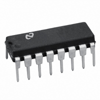
LM3524DN/NOPB National Semiconductor, LM3524DN/NOPB Datasheet - Page 17

LM3524DN/NOPB
Manufacturer Part Number
LM3524DN/NOPB
Description
IC REGULATOR PWM SWITCHER 16-DIP
Manufacturer
National Semiconductor
Type
Step-Down (Buck), Step-Up (Boost), Flybackr
Datasheet
1.LM2524DNNOPB.pdf
(22 pages)
Specifications of LM3524DN/NOPB
Internal Switch(s)
Yes
Synchronous Rectifier
No
Number Of Outputs
1
Voltage - Output
5V
Current - Output
200mA
Frequency - Switching
550kHz
Voltage - Input
8 ~ 40 V
Operating Temperature
0°C ~ 125°C
Mounting Type
Through Hole
Package / Case
16-DIP (0.300", 7.62mm)
Power - Output
1W
Lead Free Status / RoHS Status
Lead free / RoHS Compliant
Other names
*LM3524DN
LM3524DN
LM3524DN
THE STEP-UP SWITCHING REGULATOR
Figure 18 shows the basic circuit for a step-up switching reg-
ulator. In this circuit Q1 is used as a switch to alternately apply
V
energy is drawn from V
ased and I
Q1 opens, t
where D1 turns ON. The output current is now supplied
through L1, D1 to the load and any charge lost from C
t
the current through L1 has a DC component plus some ΔI
ΔI
19 shows the inductor's current in relation to Q1's ON and
OFF times.
Since ΔI
and neglecting V
The above equation shows the relationship between V
and duty cycle.
In calculating input current I
DC current, assume first 100% efficiency:
for η = 100%, P
ON
IN
L
is replenished. Here also, as in the step-down regulator,
across inductor L1. During the time, t
is again selected to be approximately 40% of I
L
+ = ΔI
o
OFF
is supplied from the charge stored in C
L
, voltage V1 will rise positively to the point
OUT
−, V
SAT
= P
IN
and V
FIGURE 19. Relation of Switch Timing to Inductor Current in Step-Up Regulator
t
ON
IN
IN
and stored in L1; D1 is reverse bi-
= V
D1
IN(DC)
o
t
OFF
, which equals the inductor's
− V
IN
t
OFF
ON
,
, Q1 is ON and
L
o
. Figure
o
. When
during
IN
, V
L
o
.
17
This equation shows that the input, or inductor, current is
larger than the output current by the factor (1 + t
this factor is the same as the relation between V
(DC)
So far it is assumed η = 100%, where the actual efficiency or
η
Q1 and forward on voltage of D1. The internal power loss due
to these voltages is the average I
through either V
loss becomes I
This equation assumes only DC losses, however η
ther decreased because of the switching time of Q1 and D1.
MAX
can also be expressed as:
FIGURE 18. Basic Step-Up Switching Regulator
will be somewhat less due to the saturation voltage of
IN(DC)
SAT
or V
(1V). η
D1
. For V
MAX
is then:
865024
SAT
L
current flowing, or I
= V
D1
= 1V this power
ON
o
/t
www.national.com
and V
OFF
MAX
). Since
865023
is fur-
IN
, I
IN
IN
,


