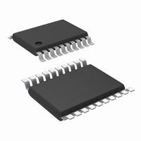
LM26003MHX/NOPB National Semiconductor, LM26003MHX/NOPB Datasheet - Page 9

LM26003MHX/NOPB
Manufacturer Part Number
LM26003MHX/NOPB
Description
IC REG BUCK SW 3A 20-TSSOP
Manufacturer
National Semiconductor
Series
PowerWise®r
Type
Step-Down (Buck)r
Datasheet
1.LM26003QMHNOPB.pdf
(20 pages)
Specifications of LM26003MHX/NOPB
Internal Switch(s)
Yes
Synchronous Rectifier
No
Number Of Outputs
1
Voltage - Output
1.25 ~ 35 V
Current - Output
3A
Frequency - Switching
150kHz ~ 500kHz
Voltage - Input
4 ~ 38 V
Operating Temperature
-40°C ~ 125°C
Mounting Type
Surface Mount
Package / Case
20-TSSOP Exposed Pad, 20-eTSSOP, 20-HTSSOP
Power - Output
3.1W
Lead Free Status / RoHS Status
Lead free / RoHS Compliant
Other names
LM26003MHX
Available stocks
Company
Part Number
Manufacturer
Quantity
Price
Company:
Part Number:
LM26003MHX/NOPB
Manufacturer:
ST
Quantity:
445
Part Number:
LM26003MHX/NOPB
Manufacturer:
TI/德州仪器
Quantity:
20 000
Operation Description
GENERAL
The LM26003 is a current mode PWM buck regulator. At the
beginning of each clock cycle, the internal high-side switch
turns on, allowing current to ramp-up in the inductor. The in-
ductor current is internally monitored during each switching
cycle. A control signal derived from the inductor current is
compared to the voltage control signal at the COMP pin, de-
rived from the feedback voltage. When the inductor current
reaches its threshold, the high-side switch is turned off and
inductor current ramps-down. While the switch is off, inductor
current is supplied through the catch diode. This cycle repeats
at the next clock cycle. In this way, duty-cycle and output volt-
age are controlled by regulating inductor current. Current
mode control provides superior line and load regulation. Other
benefits include cycle-by-cycle current limiting and a simpli-
fied compensation scheme. Typical PWM waveforms are
shown in
SLEEP MODE
In light load conditions, the LM26003 automatically switches
into sleep mode for improved efficiency. As loading decreas-
es, the voltage at FB increases and the COMP voltage de-
creases. When the COMP voltage reaches the 0.6V (typical)
clamp threshold and the FB voltage rises 1% above nominal,
sleep mode is enabled and switching stops. The regulator re-
mains in sleep mode until the FB voltage falls to the reset
threshold, at which point switching resumes. This 1% FB win-
dow limits the corresponding output ripple requirement to
approximately 1% of nominal output voltage. The sleep cycle
will repeat until load current is increased.
ical switching and output voltage waveforms in sleep mode.
Figure
FIGURE 1. PWM Waveforms
1.
1A Load, Vin = 12V
Figure 2
30067604
shows typ-
9
In sleep mode, quiescent current is reduced to less than 40
µA (typical) when not switching. The DC sleep mode thresh-
old can roughly be calculated according to the equation be-
low:
Where Imin = Ilim/16 (4.7A/16 typically) and D = duty-cycle,
defined as (Vout + Vdiode)/Vin.
When load current increases above this limit, the LM26003 is
forced back into PWM operation. The sleep mode threshold
varies with frequency, inductance, and duty-cycle as shown
in
Below the sleep threshold, decreasing load current results in
longer sleep cycles, which can be quantified as shown below:
Where Dwake is the percentage of time awake when the load
current is below the sleep threshold. Sleep mode combined
with low IQ operation minimizes the input supply current. Input
Figure
FIGURE 3. Sleep Mode Threshold vs Vin
3.
FIGURE 2. Sleep Mode Waveforms
25 mA Load, Vin = 12V
Dwake = Iload/Isleep
Vout = 3.3V
30067605
30067607
www.national.com


