LM20136MHE/NOPB National Semiconductor, LM20136MHE/NOPB Datasheet
LM20136MHE/NOPB
Specifications of LM20136MHE/NOPB


Related parts for LM20136MHE/NOPB


LM20136MHE/NOPB Summary of contents
Page 1
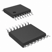
... The LM20136 is offered in a 16-pin eTSSOP package with an exposed pad that can be soldered to the PCB, eliminating the need for bulky heatsinks. Typical Application Circuit ® PowerWise is a registered trademark of National Semiconductor Corporation. © 2009 National Semiconductor Corporation LM20136 Features ■ Input voltage range 2.95V to 5.5V ■ ...
Page 2
Connection Diagram Ordering Information Order Number Package Type LM20136MH eTSSOP-16 LM20136MHE LM20136MHX Pin Descriptions Pin # Name 1 SS/TRK Soft-Start or Tracking control input. An internal 5 µA current source charges an external capacitor to set the Soft-Start ramp rate. ...
Page 3
... Absolute Maximum Ratings If Military/Aerospace specified devices are required, please contact the National Semiconductor Sales Office/ Distributors for availability and specifications. Voltages from the indicated pins to GND AVIN, PVIN, EN, PGOOD, SS/ TRK, COMP, FB, SW, SYNC Storage Temperature Junction Temperature Electrical Characteristics Limits in standard type are for T = 25° ...
Page 4
Symbol Parameter Enable V EN Pin Turn on Threshold IH_EN V EN Pin Hysteresis EN_HYS Thermal Shutdown T Thermal Shutdown SD T Thermal Shutdown Hysteresis SD_HYS Thermal Resistance θ Junction to Ambient JA Note 1: Absolute Maximum Ratings indicate limits ...
Page 5
High-Side FET resistance vs. Temperature (T Error Amplifier Gain vs. Frequency Load Regulation ) Low-Side FET resistance vs. Temperature (T J 30053967 Line Regulation 30053936 Feedback Pin Voltage vs. Temperature (T 30053938 30053968 30053937 ) J 30053951 ...
Page 6
Switching Frequency vs. Temperature (T Quiescent Current vs. Temperature (Not Switching) Enable Threshold vs. Temperature (T www.national.com ) Switch Synchronization J 30053939 Shutdown Current vs. V 30053940 ) UVLO Threshold vs. Temperature (T J 30053928 6 30053960 IN 30053941 ) ...
Page 7
Peak Current Limit vs. Temperature (T 30053969 Peak Current Limit vs 30053962 Line Transient Response ) Peak Current Limit vs Load Transient Response Start-Up (Soft-Start) 30053943 7 OUT 30053961 30053934 30053944 www.national.com ...
Page 8
Start-Up (Tracking) Short Circuit Input Current vs. V www.national.com 30053933 P IN 30053956 8 Power Down 30053932 vs. I GOOD PGOOD 30053927 ...
Page 9
Block Diagram 9 30053903 www.national.com ...
Page 10
Operation Description GENERAL The LM20136 switching regulator features all of the functions necessary to implement an efficient low voltage buck regula- tor using a minimum number of external components. This easy to use regulator features two integrated switches and is ...
Page 11
To avoid false tripping during transient glitches the PGOOD pin has 16 µs of built in deglitch time to UVLO The LM20136 has a built-in under-voltage lockout protection circuit that keeps the device from ...
Page 12
At very light loads, usually below 100mA, several pulses may be skipped in between switching cycles, effectively reducing www.national.com the switching frequency and further improving light-load effi- ciency. FIGURE 2. Modes of Operation for LM20136 12 30053905 ...
Page 13
Design Guide This section walks the designer through the steps necessary to select the external components to build a fully functional power supply. As with any DC-DC converter numerous trade- offs are possible to optimize the design for efficiency, size, ...
Page 14
Where, C (F) is the minimum required output capacitance, OUT L (H) is the value of the inductor, V voltage drop ignoring loop bandwidth considerations, ΔI (A) is the load step change, R STEP capacitor ESR, V (V) is the ...
Page 15
To achieve a -20dB/decade slope, the error amplifier zero, located should positioned to cancel the output filter Z(EA) pole ( ...
Page 16
FIGURE 7. Sequencing LM20136 with Precision Enable The value for resistor R can be selected by the user to control B the current through the divider. Typically this resistor will be selected to be between 10 kΩ and 1 MΩ. ...
Page 17
T is the ambient temperature in ° the output load current. OUT DCR is the inductor series resistance important to always keep the operating junction temper- ature (T ) below 125°C for reliable operation. If ...
Page 18
FIGURE 11. Schematic of LM20136 Highlighting Layout Sensitive Nodes www.national.com 30053922 18 ...
Page 19
... C1 as outlined in the design C1 30053901 = 500kHz) SYNC Manufacturer Qty National Semiconductor 1 TDK 1 TDK 1 TDK 1 Vishay-Dale 1 Murata 1 Murata 1 Vishay-Dale 1 Murata 1 Vishay-Vitramon 1 Vishay-Dale 1 Vishay-Dale 1000kHz) SYNC Manufacturer Qty National Semiconductor 1 TDK 1 TDK 1 TDK 1 Vishay-Dale 1 Murata 1 Murata 1 Vishay-Dale 1 Vishay-Vitramon 1 Vishay-Vitramon 1 Vishay-Dale 1 Vishay-Dale 1 www.national.com ...
Page 20
Physical Dimensions www.national.com inches (millimeters) unless otherwise noted 16-Lead eTSSOP Package NS Package Number MXA16A 20 ...
Page 21
Notes 21 www.national.com ...
Page 22
... For more National Semiconductor product information and proven design tools, visit the following Web sites at: Products Amplifiers www.national.com/amplifiers Audio www.national.com/audio Clock and Timing www.national.com/timing Data Converters www.national.com/adc Interface www.national.com/interface LVDS www.national.com/lvds Power Management www.national.com/power Switching Regulators www.national.com/switchers LDOs www.national.com/ldo LED Lighting www ...