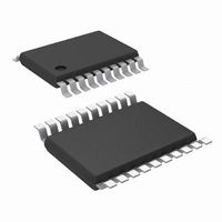
LM5005MH/NOPB National Semiconductor, LM5005MH/NOPB Datasheet

LM5005MH/NOPB
Specifications of LM5005MH/NOPB
*LM5005MH/NOPB
LM5005MH
Available stocks
Related parts for LM5005MH/NOPB
LM5005MH/NOPB Summary of contents
Page 1
... The device is available in a power enhanced TSSOP-20 package featuring an exposed die attach pad to aid thermal dissipation. Simplified Application Schematic © 2007 National Semiconductor Corporation Features ■ Integrated 75V, 2.5A N-Channel Buck Switch ■ ...
Page 2
Connection Diagram Ordering Information Order Number Package Type LM5005MH Exposed Pad TSSOP-20 LM5005MHX Exposed Pad TSSOP-20 www.national.com 20161902 Top View 20-Lead TSSOP NSC Package Drawing MXA20A MXA20A 2 Supplied As 73 Units in Rail 2500 Units on Tape and Reel ...
Page 3
Pin Descriptions Pin(S) Name 1 VCC Output of the bias regulator 2 SD Shutdown or UVLO input 3, 4 Vin Input supply voltage 5 SYNC Oscillator synchronization input or output The internal oscillator can be synchronized to an external 6 ...
Page 4
Pin(S) Name 20 BST Boost input for bootstrap capacitor NA EP Exposed Pad www.national.com Description An external capacitor is required between the BST and the SW pins. A 0.022µF ceramic capacitor is recommended. The capacitor is charged from Vcc via ...
Page 5
... Absolute Maximum Ratings If Military/Aerospace specified devices are required, please contact the National Semiconductor Sales Office/ Distributors for availability and specifications GND IN BST to GND PRE to GND SW to GND (Steady State) BST GND CC Electrical Characteristics apply over full Operating Junction Temperature range. V Symbol ...
Page 6
Symbol Parameter RAMP GENERATOR Ramp Current 1 Ramp Current 2 PWM COMPARATOR Forced Off-time Min On-time COMP to PWM Comparator Offset ERROR AMPLIFIER Feedback Voltage FB Bias Current DC Gain COMP Sink / Source Current Unity Gain Bandwidth THERMAL SHUTDOWN ...
Page 7
Soft Start Current vs Temperature 20161922 7kΩ L 20161924 Demoboard Efficiency vs I and V OUT IN 20161926 12V IN Error Amplifier Gain/Phase A = 101 ...
Page 8
Typical Application Circuit and Block Diagram www.national.com 8 ...
Page 9
Detailed Operating Description The LM5005 high voltage switching regulator features all of the functions necessary to implement an efficient high voltage buck regulator using a minimum of external components. This easy to use regulator integrates a 75V N-Channel buck switch ...
Page 10
Shutdown / Standby The LM5005 contains a dual level Shutdown (SD) circuit. When the SD pin voltage is below 0.7V, the regulator low current shutdown mode. When the SD pin voltage is greater than 0.7V but less ...
Page 11
FIGURE 5. Simplified Oscillator Block Diagram and SYNC I/O Circuit Error Amplifier and PWM Comparator The internal high gain error amplifier generates an error signal proportional to the difference between the regulated output voltage and an internal precision reference (1.225V). ...
Page 12
The Sample and Hold DC level illustrated in Figure 6. is de- rived from a measurement of the re-circulating Schottky diode anode current. The re-circulating diode anode should be con- nected to the IS pin. The diode current flows through ...
Page 13
Current Limit The LM5005 contains a unique current monitoring scheme for control and over-current protection. When set correctly, the emulated current sense signal provides a signal which is pro- portional to the buck switch current with a scale factor of ...
Page 14
Application Information EXTERNAL COMPONENTS The procedure for calculating the external components is il- lustrated with the following design example. The Bill of Mate- rials for this design is listed in Table1. The circuit shown in Figure 1 is configured for ...
Page 15
RMS current rating and minimum ripple voltage. A good approximation for the re- quired ripple current rating necessary is I Quality ceramic capacitors with a low ESR should be selected for the input filter. To ...
Page 16
Components R4 and C5 configure the error amplifier as a type II configuration which has a pole at unity and a zero at f (2πR4C5). The error amplifier zero cancels the modulator pole leaving a single pole response at the ...
Page 17
FIGURE 12. VCC Bias from VOUT for 8V < VOUT < 14V FIGURE 13. VCC Bias with Additional Winding on the Output Inductor 17 20161918 20161919 www.national.com ...
Page 18
... NOT USED DIODE, 100V, CENTRAL DIODE, 100V, IR (D1-ALT) INDUCTOR, COOPER NOT USED NOT USED RESISTOR RESISTOR RESISTOR RESISTOR RESISTOR REGULATOR, NATIONAL SEMICONDUCTOR 1.1, where R is OUT VALUE 2.2µ, 100V 2.2µ, 100V 330p, 100V 0.01µ, 100V 0.01µ, 100V 0.022µ ...
Page 19
PCB Layout Component Side Solder Side Silkscreen 19 20161929 20161930 20161931 www.national.com ...
Page 20
Physical Dimensions www.national.com inches (millimeters) unless otherwise noted 20-Lead TSSOP Package NS Package Number MXA20A 20 ...
Page 21
Notes 21 www.national.com ...
Page 22
... National Semiconductor and the National Semiconductor logo are registered trademarks of National Semiconductor Corporation. All other brand or product names may be trademarks or registered trademarks of their respective holders. ...


