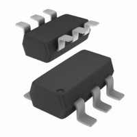
MAX1720EUTG ON Semiconductor, MAX1720EUTG Datasheet

MAX1720EUTG
Specifications of MAX1720EUTG
Available stocks
Related parts for MAX1720EUTG
MAX1720EUTG Summary of contents
Page 1
... PIN CONNECTIONS V out V in −V out C− ORDERING INFORMATION Device MAX1720EUT MAX1720EUTG †For information on tape and reel specifications, including part orientation and tape sizes, please refer to our Tape and Reel Packaging Specifications Brochure, BRD8011/D. 1 http://onsemi.com TSOP−6 SN SUFFIX CASE 318G 1 ...
Page 2
MAXIMUM RATINGS* Rating Á Á Á Á Á Á Á Á Á Á Á Á Á Á Á Á Á Á Input Voltage Range (V to GND) in Á Á Á Á Á Á Á Á Á Á Á Á ...
Page 3
Figure 14 Test Setup 25° 1.0 1.5 2.0 2.5 3.0 3 SUPPLY VOLTAGE (V) in Figure 2. Output Resistance vs. Supply Voltage ...
Page 4
Figure 14 Test Setup 2 −1 3.3 V −2.0 in −3.0 −4.0 −5.0 −6 OUTPUT CURRENT (mA) out Figure 8. Output Voltage vs. Output Current ...
Page 5
OSC Figure 14. Test Setup/Voltage Inverter DETAILED OPERATING DESCRIPTION The MAX1720 charge pump converter inverts the voltage applied ...
Page 6
Capacitor Selection In order to maintain the lowest output resistance and output ripple voltage recommended that low ESR capacitors be used. Additionally, larger values of C lower the output resistance and larger values of C reduce output voltage ...
Page 7
The MAX1720 primary function is a voltage inverter. The device will convert 5.0 V into −5.0 V with light loads. Two capacitors are required for the inverter to function. A third capacitor, the input bypass capacitor, may be required depending ...
Page 8
Figure 22. Negative Output Voltage Doubler A single device can be used to construct a negative voltage doubler. The output voltage is approximately equal to −2V the forward voltage drop of each external diode. The performance characteristics ...
Page 9
A single device can be used to construct a negative voltage tripler. The output voltage is approximately equal to −3V the forward voltage drop of each external diode. The performance characteristics for the above converter are shown below. Note that ...
Page 10
Capacitors = single device can be used to construct a positive voltage tripler. The output voltage is approximately equal to 3V the forward voltage drop of each external diode. The performance ...
Page 11
A zener diode can be used with the shutdown input to provide closed loop regulation performance. This significantly reduces the converter’s output resistance and dramatically enhances the load regulation. For closed loop operation, the desired regulated output voltage must be ...
Page 12
An adjustable shunt regulator can be used with the shutdown input to give excellent closed loop regulation performance. The shunt regulator acts as a comparator with a precise input offset voltage which significantly reduces the converter’s output resistance and dramatically ...
Page 13
An increase in converter output current capability with a reduction in output resistance can be obtained by paralleling two or more devices. The output current capability is approximately equal to the number of devices paralleled. A single shared output capacitor ...
Page 14
Figure 39. Line and Load Regulated Negative Output Voltage This converter is a combination of Figures 37 and 32. It provides a line and load regulated output of −2. ...
Page 15
The MAX1720 can be configured to produce a positive output voltage doubler with current capability in excess of 500 mA. This is accomplished with the addition of two external switch transistors and two Schottky diodes. The output voltage is approximately ...
Page 16
single device can be used to split a negative input voltage. The output voltage is approximately equal to −V performance characteristics are shown below. Note that the converter has an output resistance −1.5 −1.7 ...
Page 17
All of the previously shown converter circuits have only single outputs. Applications requiring multiple outputs can be constructed by incorporating combinations of the former circuits. The converter shown above combines Figures 26 and 32 to form a regulated negative output ...
Page 18
... Pb−Free strategy and soldering details, please download the ON Semiconductor Soldering and Mounting Techniques Reference Manual, SOLDERRM/D. ON Semiconductor and are registered trademarks of Semiconductor Components Industries, LLC (SCILLC). SCILLC reserves the right to make changes without further notice to any products herein ...


