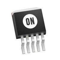
LM2575D2T-5R4G ON Semiconductor, LM2575D2T-5R4G Datasheet - Page 3

LM2575D2T-5R4G
Manufacturer Part Number
LM2575D2T-5R4G
Description
IC REG SW 1A 5V STEPDWN D2PAK
Manufacturer
ON Semiconductor
Type
Step-Down (Buck)r
Datasheet
1.LM2575T-5G.pdf
(28 pages)
Specifications of LM2575D2T-5R4G
Internal Switch(s)
Yes
Synchronous Rectifier
No
Number Of Outputs
1
Voltage - Output
5V
Current - Output
1A
Frequency - Switching
52kHz
Voltage - Input
4.75 ~ 40 V
Operating Temperature
-40°C ~ 125°C
Mounting Type
Surface Mount
Package / Case
D²Pak, TO-263 (5 leads + tab)
Mounting Style
SMD/SMT
Lead Free Status / RoHS Status
Lead free / RoHS Compliant
Power - Output
-
Lead Free Status / Rohs Status
Lead free / RoHS Compliant
Other names
LM2575D2T-5R4G
LM2575D2T-5R4GOSTR
LM2575D2T-5R4GOSTR
Available stocks
Company
Part Number
Manufacturer
Quantity
Price
Part Number:
LM2575D2T-5R4G
Manufacturer:
ON/安森美
Quantity:
20 000
1. External components such as the catch diode, inductor, input and output capacitors can affect switching regulator system performance.
2. Tested junction temperature range for the LM2575 and the NCV2575:
OPERATING RATINGS
specific performance limits. For guaranteed specifications and test conditions, see the Electrical Characteristics.)
SYSTEM PARAMETERS
ELECTRICAL CHARACTERISTICS
for the 12 V version, and V
operating junction temperature range that applies [Note 2], unless otherwise noted.)
LM2575−3.3 (Note 1 Test Circuit Figure 14)
LM2575−5 ([Note 1] Test Circuit Figure 14)
LM2575−12 (Note 1 Test Circuit Figure 14)
LM2575−15 (Note 1 Test Circuit Figure 14)
LM2575 ADJUSTABLE VERSION (Note 1 Test Circuit Figure 14)
Operating Junction Temperature Range
Supply Voltage
Output Voltage (V
Output Voltage (4.75 V ≤ V
Efficiency (V
Output Voltage (V
Output Voltage (8.0 V ≤ V
Output Voltage (V
Output Voltage (15 V ≤ V
Efficiency (V
Output Voltage (V
Output Voltage (18 V ≤ V
Efficiency (V
Feedback Voltage (V
Feedback Voltage (8.0 V ≤ V
Efficiency (V
T
T
T
T
Efficiency (V
T
T
T
T
T
T
When the LM2575 is used as shown in the Figure 14 test circuit, system performance will be as shown in system parameters section.
J
J
J
J
J
J
J
J
J
J
= −40 to +125°C
= −40 to +125°C
= 25°C
= −40 to +125°C
= 25°C
= −40 to +125°C
= 25°C
= −40 to +125°C
= 25°C
= 25°C
in
in
in
in
in
= 12 V, I
= 12 V, I
= 15V, I
= 18 V, I
= 12 V, I
in
in
in
in
= 30 V, I
= 12 V, I
= 12 V, I
= 25 V, I
in
Load
Load
Load
Load
= 12 V, I
Load
in
in
in
in
(Operating Ratings indicate conditions for which the device is intended to be functional, but do not guarantee
in
≤ 40 V, 0.2 A ≤ I
= 1.0 A)
≤ 40 V, 0.2 A ≤ I
= 1.0 A)
= 1.0 A)
= 1.0 A, V
≤ 40 V, 0.2 A ≤ I
= 30 V for the 15 V version. I
Load
Load
Load
Load
Characteristics
= 1.0 A)
in
≤ 40 V, 0.2 A ≤ I
≤ 40 V, 0.2 A ≤ I
Load
([Note 1] Test Circuit Figure 14)
= 0.2 A, T
= 0.2 A, T
= 0.2 A, T
= 0.2 A, T
= 0.2 A, V
out
Rating
= 5.0 V)
(Unless otherwise specified, V
J
J
J
J
Load
Load
Load
= 25°C)
= 25°C)
= 25°C)
= 25°C)
Load
out
Load
≤ 1.0 A)
≤ 1.0 A)
≤ 1.0 A)
= 5.0 V, T
≤ 1.0 A)
≤ 1.0 A, V
http://onsemi.com
Load
J
= 25°C)
out
= 200 mA. For typical values T
= 5.0 V)
3
in
= 12 V for the 3.3 V, 5.0 V, and Adjustable version, V
T
Symbol
low
V
V
V
V
V
V
V
V
V
V
out
out
η
η
η
η
η
out
out
out
out
out
out
FB
FB
= −40°C
Symbol
3.234
3.168
3.135
14.25
1.193
11.52
11.76
1.217
4.75
11.4
14.4
1.18
J
Min
14.7
4.8
4.9
V
= 25°C, for min/max values T
T
−
−
−
−
−
in
J
T
high
= +125°C
1.23
Typ
1.23
3.3
3.3
5.0
5.0
12
15
75
77
12
88
15
88
77
−
−
−
−
−
−40 to +125
Value
40
3.366
3.432
3.465
12.48
15.75
1.267
12.24
1.243
Max
5.25
12.6
15.6
1.28
15.3
5.2
5.1
−
−
−
−
−
J
is the
in
= 25 V
Unit
Unit
°C
V
V
V
%
%
%
%
%
V
V
V
V
V
V
V
V


