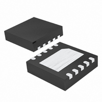
MAX8815AETB+T Maxim Integrated Products, MAX8815AETB+T Datasheet - Page 10

MAX8815AETB+T
Manufacturer Part Number
MAX8815AETB+T
Description
IC DC/DC CONV STP UP 10TDFN-EP
Manufacturer
Maxim Integrated Products
Type
Step-Up (Boost)r
Datasheet
1.MAX8815AETBT.pdf
(15 pages)
Specifications of MAX8815AETB+T
Internal Switch(s)
Yes
Synchronous Rectifier
Yes
Number Of Outputs
1
Voltage - Output
3.3 ~ 5 V
Current - Output
1A
Frequency - Switching
2MHz
Voltage - Input
1.2 ~ 5.5 V
Operating Temperature
-40°C ~ 85°C
Mounting Type
Surface Mount
Package / Case
10-TDFN Exposed Pad
Power - Output
1.48W
Lead Free Status / RoHS Status
Lead free / RoHS Compliant
1A, 97% Efficiency, 30µA Quiescent Current
Step-Up Converter with True Shutdown
The MAX8815A uses a current-mode PWM control
scheme. The voltage difference between FB and an
internal 1.265V (typ) reference generates an error sig-
nal that programs the peak inductor current to regulate
the output voltage. The default peak-inductor current
limit is 2.5A (typ). Inductor current is sensed across the
internal switch and summed with a slope-compensation
signal. The PWM comparator compares this summed
signal to the error-amplifier output. At the beginning of
each clock cycle, the n-channel switch turns on until
the PWM comparator trips. During this time, inductor
current ramps up, storing energy in its magnetic field.
When the n-channel switch turns off, the internal syn-
chronous p-channel rectifier turns on. The inductor
releases the stored energy as the current ramps down
and provides energy to the output. The MAX8815A
operates in two modes, normal mode and FPWM mode,
depending on the voltage at SKIPB.
Drive SKIPB low to select the normal mode of opera-
tion. In this mode, the device operates in PWM only
when driving medium to heavy loads. As the load cur-
rent decreases and crosses the low-power idle-mode
threshold, the PWM comparator and oscillator are dis-
abled. In this low-power mode, switching occurs only
as needed to service the output. This improves the effi-
ciency for light loads, and the device consumes only
30µA under no-load conditions. The threshold for enter-
ing skip mode is approximately 90mA load with a 3.6V
input and 5V output. When switching in normal mode,
the inductor current terminates at zero for each switch-
ing cycle.
Drive SKIPB high to select the MAX8815A’s FPWM
mode of operation. The IC switches at a constant fre-
quency (2MHz) and modulates the MOSFET switch
pulse width to control the power transferred per cycle
to regulate the output voltage. Switching harmonics
generated by fixed-frequency operation are consistent
and easily filtered. This is important in noise-sensitive
applications.
The MAX8815A does not allow for dynamic switching
between normal and FPWM modes.
10
______________________________________________________________________________________
DC-DC Converter
Normal Mode
FPWM Mode
The MAX8815A matches the load regulation to the volt-
age droop seen during load transients. This is some-
times called voltage positioning. Benefits include lower
peak-to-peak output-voltage deviation for a given load
step without requiring an increase in filter load capaci-
tance. There is minimal voltage droop when transition-
ing from light load to full load and minimum overshoot
when going from full load to light load.
The term “positioning” refers to setting the output volt-
age to a level that is dependent on load current (Figure
2). At minimum load, the output voltage is set to a
slightly higher than nominal level. At full load, the output
voltage is slightly lower than the nominal level. With
voltage positioning, the total voltage deviation during a
transient is significantly improved over traditional high-
gain control loops. Traditional high-gain loops use inte-
grators that maximize gain at low frequencies to
provide tight DC-load regulation; however, due to the
capacitive element in the feedback loop, these high-
gain amplifiers typically take hundreds of microsec-
onds to respond to a load step and return to steady
state. As a result, the voltage can droop by as much as
6% or more during the recovery time. In portable equip-
ment where the output load can change frequently and
the amount of output capacitance is limited, this can
result in a wide short-term output fluctuation (Figure 3).
Voltage positioning on the MAX8815A allows up to 3%
(typ) of load regulation and no further transient droop
(Figures 2 and 3). Thus, during load transients the volt-
age delivered remains within specification more effec-
tively than other regulators that might have tighter DC
accuracy. In systems with high-speed CPUs, thou-
sands of system clock cycles can occur during the time
it takes a traditional high-gain loop to respond to a load
step. Consequently, 3% load regulation with no tran-
sient droop is better suited to such systems than a
power supply that may specify 1% DC-load regulation,
but then exhibits 6% or more of transient droop during
load steps (see the Load Transient graph in the Typical
Operating Characteristics section).
Load-Transient Response/
Voltage Positioning


