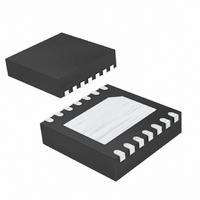
MAX8627ETD+T Maxim Integrated Products, MAX8627ETD+T Datasheet - Page 2

MAX8627ETD+T
Manufacturer Part Number
MAX8627ETD+T
Description
IC CONV BOOST SYNC 14-TDFN
Manufacturer
Maxim Integrated Products
Type
Step-Up (Boost)r
Datasheet
1.MAX8627ETDT.pdf
(14 pages)
Specifications of MAX8627ETD+T
Internal Switch(s)
Yes
Synchronous Rectifier
Yes
Number Of Outputs
1
Voltage - Output
3 ~ 5 V
Current - Output
1A
Frequency - Switching
1MHz
Voltage - Input
0.9 ~ 5.5 V
Operating Temperature
-40°C ~ 85°C
Mounting Type
Surface Mount
Package / Case
14-TDFN Exposed Pad
Power - Output
1.45W
Lead Free Status / RoHS Status
Lead free / RoHS Compliant
ABSOLUTE MAXIMUM RATINGS
OUTS, BATT to GND ................................................-0.3V to +6V
LX Current (Note 1) ...............................................................3.5A
AGND, PG to GND ................................................-0.3V to +0.3V
POUT to OUTS ......................................................-0.3V to +0.3V
FB, ILIM, ON to
Low V
Boost Converter with True Shutdown
Stresses beyond those listed under “Absolute Maximum Ratings” may cause permanent damage to the device. These are stress ratings only, and functional
operation of the device at these or any other conditions beyond those indicated in the operational sections of the specifications is not implied. Exposure to
absolute maximum rating conditions for extended periods may affect device reliability.
ELECTRICAL CHARACTERISTICS
(V
noted.)
Dual Mode is a trademark of Maxim Integrated Products, Inc.
2
Note 1: LX has internal clamp diodes to the IC internal power node V
Applications that forward bias these diodes should take care not to exceed the device’s power-dissipation limits.
GENERAL
Operating Input Voltage Range
Minimum Startup Voltage
Maximum Startup Current Limit
Supply Current
OSCILLATOR
Switching Frequency
Startup Switching Frequency
Maximum Duty Cycle
Output Voltage Adjust Range
FB Regulation Voltage
FB Load Regulation
FB Line Regulation
FB Input Leakage Current
ILIM Dual Mode™ Threshold
Idle Mode Trip Level
DC-DC SWITCHES
n-Channel On-Resistance
p-Channel On-Resistance
Damping Switch On-Resistance
n-Channel Current limit
GND.....0.3V to the higher of (V
OUTS
_______________________________________________________________________________________
= V
PARAMETER
POUT
BATT
= 5V, V
ON
= V
, 20µA IQ, 1MHz Synchronous
OUTS
BATT
+ 0.3V) and (V
(Note 1)
No load (Note 1)
Shutdown, ON = GND
No load, no switching
No load, switching
No load
0A to 1A output current load step
V
V
V
Low level
High level
(Note 3)
V
V
= 3.6V, V
BATT
FB
OUTS
ILIM
ILIM
= 1.2V,
= 0V
= 0.6V
= 2.7V to 3V, output current = 0.5A
= V
ILIM
POUT
BATT
= GND, T
= V
+ 0.3V)
BATT
CONDITIONS
A
= 5.5V T
= -40°C to +85°C, typical values are at T
Continuous Power Dissipation (T
Operating Temperature Range ...........................-40°C to +85°C
Junction Temperature ......................................................+150°C
Storage Temperature Range .............................-65°C to +150°C
Lead Temperature (soldering, 10s) .................................+300°C
T
T
T
T
T
14-Pin TDFN 3mm x 3mm
(derate 18.2mW/°C above +70°C) .............................1454mW
A
A
A
A
A
A
PWR
= +25°C
= +85°C
= 0°C to +85°C
= -40°C (Note 2)
= +25°C
= +85°C
(where V
PWR
is the higher of BATT or POUT) and PG.
1.005
MIN
0.95
82.5
0.45
-50
0.9
3.0
3.2
A
= +70°C)
A
1.015
=
TYP
87.0
+20
0.15
0.15
1.2
0.5
0.1
0.2
1.0
2.0
-30
-10
-10
3.5
1.0
20
20
20
50
17
+25°C, unless otherwise
1.025
MAX
1.05
0.25
0.25
0.25
+50
5.5
1.5
5.2
3.7
30
35
30
1
UNITS
mV/A
MHz
MHz
mV
mA
µA
nA
%
Ω
Ω
Ω
V
V
A
V
V
V
A


