NCP3163PWG ON Semiconductor, NCP3163PWG Datasheet - Page 3
NCP3163PWG
Manufacturer Part Number
NCP3163PWG
Description
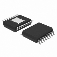
IC REG SW DC/DC 3.4A 16SOIC
Manufacturer
ON Semiconductor
Type
Step-Down (Buck), Step-Up (Boost), Invertingr
Datasheet
1.NCP3163BMNR2G.pdf
(20 pages)
Specifications of NCP3163PWG
Internal Switch(s)
Yes
Synchronous Rectifier
No
Number Of Outputs
1
Voltage - Output
Adj to 40V
Current - Output
3.4A
Frequency - Switching
50kHz ~ 300kHz
Voltage - Input
2.5 ~ 40 V
Operating Temperature
0°C ~ 70°C
Mounting Type
Surface Mount
Package / Case
16-SOIC (7.5mm Width) Exposed Pad, 16-eSOIC, 16-HSOIC
Output Voltage
1 V to 40 V
Output Current
3.4 A
Input Voltage
2.5 V to 40 V
Switching Frequency
50 KHz to 1 MHz
Operating Temperature Range
- 40 C to + 85 C
Mounting Style
SMD/SMT
Lead Free Status / RoHS Status
Lead free / RoHS Compliant
Power - Output
-
Lead Free Status / Rohs Status
Lead free / RoHS Compliant
Available stocks
Company
Part Number
Manufacturer
Quantity
Price
Company:

Part Number:
NCP3163PWG
Manufacturer:
ON
Quantity:
141


Stresses exceeding Maximum Ratings may damage the device. Maximum Ratings are stress ratings only. Functional operation above the
Recommended Operating Conditions is not implied. Extended exposure to stresses above the Recommended Operating Conditions may affect
device reliability.
1. This device series contains ESD protection and exceeds the following tests:
2. This device contains latch−up protection and exceeds 100 mA per JEDEC Standard JESD78.
3. Maximum package power dissipation limits must be observed. Maximum Junction Temperature must not be exceeded.
4. The pins which are not defined may not be loaded by external signals.
MAXIMUM RATINGS
Thermal Characteristics
Voltage Feedback 2
Voltage Feedback 1
Power Supply Voltage
Switch Collector Voltage Range
Switch Emitter Voltage Range
Switch Collector to Emitter Voltage
Switch Current
Driver Collector Voltage (Pin 8)
Driver Collector Current (Pin 8)
Bootstrap Input Current Range
Current Sense Input Voltage Range
Feedback and Timing Capacitor Input Voltage Range
Low Voltage Indicator Output Voltage Range
Low Voltage Indicator Output Sink Current
Storage Temperature Range
Maximum Junction Temperature
Operating Ambient Temperature (Note 3)
NCV3163
Timing Capacitor
Thermal Resistance, Junction−to−Case
Thermal Resistance, Junction−to−Air
NCP3163
NCP3163B
Human Body Model 2000 V per MIL−STD−883, Method 3015.
Machine Model Method 200 V.
Charged Device Model 750 V for corner pins and 500 V for others (according to AEC−Q100).
LVI Output
I
pk
Sense
GND
V
N/C
Power Dissipation and Thermal Characteristics
CC
1
2
3
4
5
6
7
8
(Note 1)
(Top View)
Rating
16
15
14
13
12
10
11
9
Bootstrap Input
Driver Collector
Switch
Emitter
N/C
Switch Collector
PIN CONNECTIONS
http://onsemi.com
3
Timing Capacitor
Switch Collector
Switch Collector
Switch Collector
Switch Collector
Driver Collector
I
pk
Sense
V
N/C
CC
Symbol
V
Note: Pin 18 must be tied to EP Flag on PCB
V
V
T
V
V
IPKSNS
R
R
I
V
V
I
CESW
I
T
I
CLVI
CSW
ESW
BST
V
Jmax
CLVI
T
SW
CC
qJC
qJA
CC
CC
stg
in
A
1
2
3
4
5
6
7
8
9
(V
EP Flag
CC
GND
− 7.0) to (V
−100 to +100
−1.0 to +7.0
−65 to +150
−40 to +125
−1.0 to +40
−2.0 to +40
−1.0 to +40
−1.0 to +40
−40 to +85
0 to +40
0 to +70
Value
+150
+40
150
3.4
10
15
56
18
17
16
15
14
13
12
10
11
CC
+ 1.0)
GND
Voltage Feedback 1
Voltage Feedback 2
LVI Output
Bootstrap Input
Switch Emitter
Switch Emitter
Switch Emitter
Switch Emitter
°C/W
Unit
mA
mA
mA
°C
°C
°C
V
V
V
V
A
V
V
V
V
Related parts for NCP3163PWG
Image
Part Number
Description
Manufacturer
Datasheet
Request
R

Part Number:
Description:
3.4 A, Stepup/down/inverting 50300 Khz Switching Regulator
Manufacturer:
ON Semiconductor
Datasheet:

Part Number:
Description:
EVAL BOARD FOR NCP3163BST
Manufacturer:
ON Semiconductor
Datasheet:

Part Number:
Description:
EVAL BOARD FOR NCP3163INV
Manufacturer:
ON Semiconductor
Datasheet:
Part Number:
Description:
ON Semiconductor [VOLTAGE REGULATOR]
Manufacturer:
ON Semiconductor
Datasheet:
Part Number:
Description:
357-036-542-201 CARDEDGE 36POS DL .156 BLK LOPRO
Manufacturer:
ON Semiconductor
Datasheet:
Part Number:
Description:
357-036-542-201 CARDEDGE 36POS DL .156 BLK LOPRO
Manufacturer:
ON Semiconductor
Datasheet:
Part Number:
Description:
357-036-542-201 CARDEDGE 36POS DL .156 BLK LOPRO
Manufacturer:
ON Semiconductor
Datasheet:
Part Number:
Description:
357-036-542-201 CARDEDGE 36POS DL .156 BLK LOPRO
Manufacturer:
ON Semiconductor
Datasheet:
Part Number:
Description:
357-036-542-201 CARDEDGE 36POS DL .156 BLK LOPRO
Manufacturer:
ON Semiconductor
Datasheet:
Part Number:
Description:
357-036-542-201 CARDEDGE 36POS DL .156 BLK LOPRO
Manufacturer:
ON Semiconductor
Datasheet:
Part Number:
Description:
357-036-542-201 CARDEDGE 36POS DL .156 BLK LOPRO
Manufacturer:
ON Semiconductor
Datasheet:
Part Number:
Description:
357-036-542-201 CARDEDGE 36POS DL .156 BLK LOPRO
Manufacturer:
ON Semiconductor
Datasheet:
Part Number:
Description:
357-036-542-201 CARDEDGE 36POS DL .156 BLK LOPRO
Manufacturer:
ON Semiconductor
Datasheet:
Part Number:
Description:
357-036-542-201 CARDEDGE 36POS DL .156 BLK LOPRO
Manufacturer:
ON Semiconductor
Datasheet: